
In a previous article, I showed how to set up and tweak performance of a silicon Fuzz Face on a solderless breadboard. The next logical step is to commit to a soldered build on perfboard or printed circuit board and house the effect in a gig-worthy enclosure. I'll show you how to do that in this article. If you bought the breadboarding kit, most of the parts can be re-used if you wish. I called this a "Bare Bones" version because it's strictly a basic Fuzz Face--no tone stack or other mods, just true-bypass switching, DC power jack and in-use LED.
For first-time builders who may not have a full set of tools, a pre-drilled enclosure is available in my store. Also, while this article is not meant to be a design manual for stompboxes, I'll anticipate some questions, talk briefly about the process I went through to get to a finished pedal and describe some of the steps in the learning curve.
Breadboard To Box - What Is Involved?
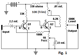
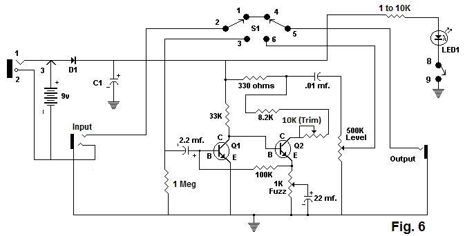
If you followed the breadboard build to its end, you have a working circuit, complete from input to output something like this:
3PDT True-Bypass Switching With In-Use LED - How It Works
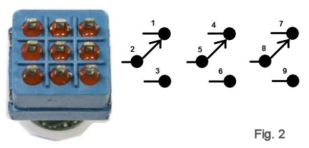
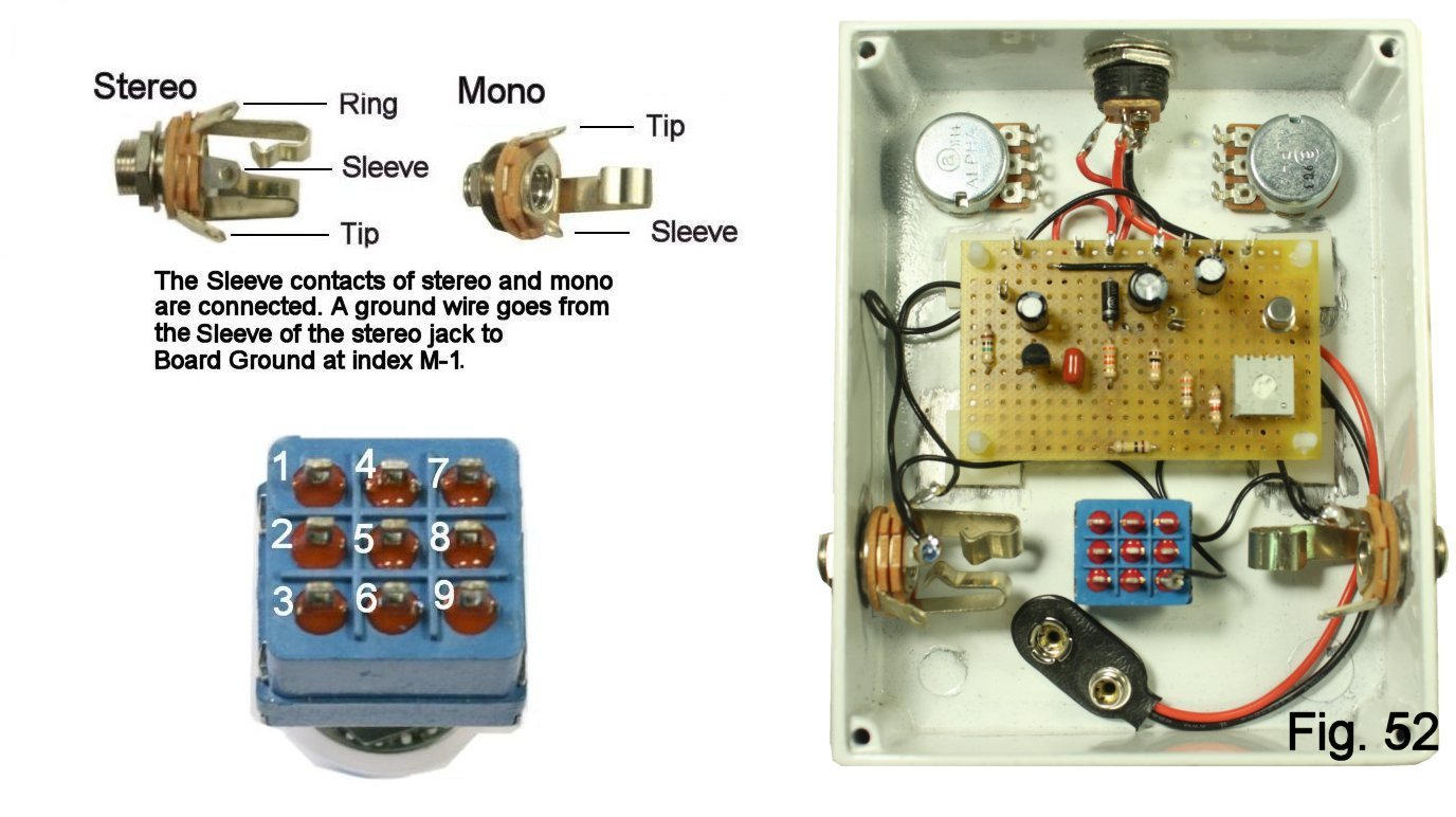
Figure 2 shows a bottom view of a typical 3PDT (Three-pole, Double-throw) footswitch. It has nine contacts, and they work as shown in the schem. Push/release once and the moving contacts (2, 5 and 8) connect to #3, #6 and #9. Push/release again and they go back. We call this a "latching" or "alternate-action" switch, because the contacts remain in their new position when you release the switch.
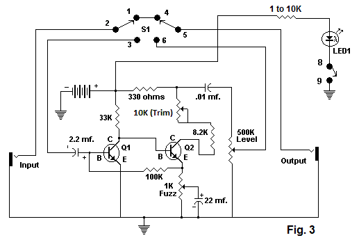
Figure 3 shows the switch added to the schematic of the effect. Let's trace through the connections and see how the switching works in practice. In the schem, the effect is bypassed. The guitar input goes from the moving contact, pin 2, through stationary contacts pin 1 and pin 4 (which are connected with a jumper) to moving contact pin 5 and then to the output jack When the switch is stomped, the input jack sees the effect input through pin 3, and the output jack sees the level control through pin 6. Two contacts of the third pole switch the LED on and off.
There are other ways to wire a stomp switch, with and without an in-use LED. They will all work, though some may be more suitable than others in a particular design situation. If you want more information, check the Beginner FAQ at diystompboxes.com, or other on-line sources.
Power
While we were on the breadboard, we switched power by disconnecting the battery. That won't work in a pedal, so we have to make some arrangements. And there are several issues:
-
We want a DC power jack, which the original Fuzz Face did not have. And we want the battery to be cut off when an external power supply is plugged in.
-
We want the circuit to be protected from reverse connection of power.
-
We want battery power to be cut off when the guitar plug is removed from the input jack.
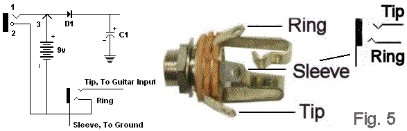
Most modern pedals accomplish all of this in the same way. External power comes in through a jack like the one in the Figure 4. This one is designed to be mounted on a panel, while others mount on a circuit board. The typical schematic is shown on the right.
Contact #1 connects to the shell of the power plug, which will be positive in the typical negative-ground pedal design. Contact #3 forms a normally-closed switch with contact #1; it shorts to #1 until a power plug is inserted. Contact #2 is the center pin, which will be ground in this configuration.
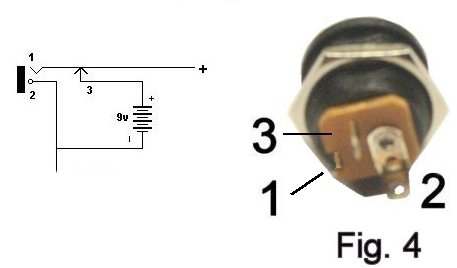
Diode D1 takes care of reverse polarity protection; it will block current flow if the battery or power supply is connected incorrectly. Capacitor C1 is called a "decoupling capacitor". It is added to help the circuit be more stable on a pedal board in which multiple pedals are being driven from one power supply. All of this is shown in Figure 5.
How Did You Get To The Mechanical Design??
This is complicated, and a full presentation is best left to people who have done it for a living, like R. G. Keen. In his case, he wrote a book about it. However, I hope that my suggestions here will be a partial "road map" that points some beginners toward planning in advance and learning to use software design tools.
Once a design has been proven on the breadboard, the first considerations for turning it into a pedal are mechanical, and they concern the off-board components and overall size of the circuit board:
How many pots?
How many switches?
In-use LED(s)?
How many jacks?
How many components on the board and what size(s)?
The answers to these questions will dictate the size and type of enclosure needed. Most DIYers will not be making an enclosure, so the next step is to pick a standard, off-the-shelf size. While there are other choices of materials, cast aluminum is very durable, and demand has made it inexpensive and widely available.
Based on the answers to the above questions (and a good deal of experience), I could have chosen to "shrink" this design into something that would fit in a "B-size" (4.39" x 2.36" x 1.03) box. However, I knew that this would be a first-build for many people, and I wanted the box to be roomy enough for a beginner to work in comfortably. I settled on the standard "BB-size" (4.7" x 3.7" x 1.18").
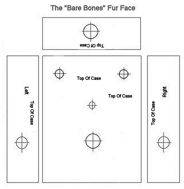
The next step is planning where the controls, switches and jacks will go. There is now a lot of on-line help for doing this. Numerous DIY sites, including SBE, of course, offer plans for finished pedals that include downloadable drilling templates for standard enclosure sizes. I didn't have a "stock" set of templates for a two-knob, two jack, one-stomp enclosure when I started the Fur Face, so I drew what I wanted using Jasc Paint Shop. Other people use MS Paint, Corel Draw or Photoshop to get to the same place. You can download from here the template file that I came up with.
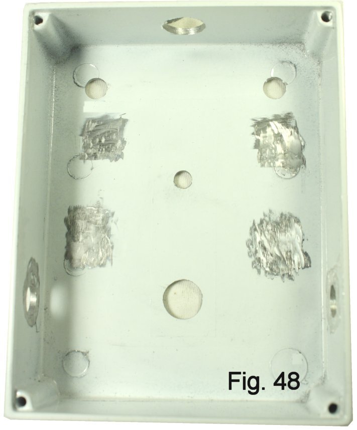
Once the positions of the off-board components have been established, the maximum size of the board that will fit in the enclosure will be clear. I picked a stock size of pad-per-hole, 306 holes, 2.375 x 1.438", that fits neatly. At this point, before I plan a board layout, I drill the enclosure and then "mock-up" the mechanical layout, both to be sure that everything will fit and so that I know that components will not bump into each other when the pedal is assembled.
Designing The Board
Please don't struggle with pencil and graph paper to locate components; the repeated place-and-try that is the essence of board design is difficult enough without having to rubber-erase and re-do. Today, there are purpose-designed CAD programs, some relatively beginner-friendly, that are optimized for board layout. I strongly suggest going this route if you are at all serious about doing your own designs. The learning curve is steep, but very satisfying. A limited-size, but fully-functional, version of EAGLE CAD, which I use, can be downloaded from http://www.cadsoftusa.com. While packages like EAGLE are specifically geared to creating printed circuit boards, the layout functions are also applicable to creating perfboard designs. For a package that's more beginner-friendly and purpose-designed for working on perfboard or stripboard, check out DIY Layout Creator. It's freeware, and absolutely marvelous (Figure 10)!
I noted earlier that the available space in the enclosure and the positions of the off-board parts dictate the size of the board. Having established all of that, I used the CAD software to draw an actual-size outline of the board. The positions of the controls and the input and output jacks dictate where the input and output on the board will be. From there, designing the layout is an enormous amount of place-and-try to get to something that you want to commit to solder. For a (Very) detailed discussion of good design rules and best practices, check out R. G. Keen's book.
Now that I have given you a look at the functioning of my bearish mind...
Let's Build The Pedal!
FAQ: I did the breadboard build and have all of those parts. What else do I need?
Here's a shopping list:
| 1 | "BB"-size Enclosure Undrilled | 0300AA |
| 1 | 3PDT stomp switch | 0200 |
| 2 | Knobs for 1/4" shaft | Your Choice |
| 4 | Self-adhesive Standoffs | 0415M |
| 1 | Pad-per-hole perfboard | 0355 |
| 9 | Push-in Terminals | 0400C |
| Bare tinned wire | 0509 | |
| Hookup Wire | 0508B1 |
If you want a pre-drilled enclosure, order SKU 0300AAB.
If you are tooling your own enclosure, download the template file and print out the templates.
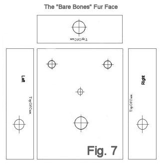
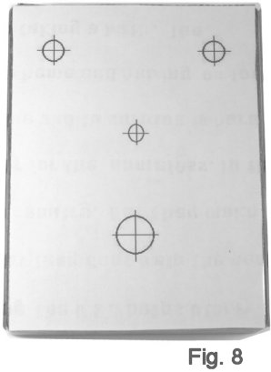
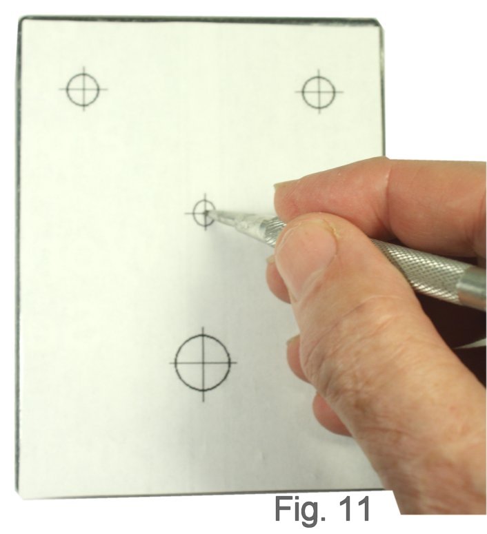
Remove the four screws that secure the lid to the enlosure. With a good, sharp scissor, cut out the template for the top. Attach a couple of pieces of double-sided clear or masking tape to the box, and carefully center the template to the cover. In the same way, attach the templates for sides, being careful to get the holes for the jacks in the correct locations relative to the the switch. The output jack is on the left as you look at the front of the pedal and input is on the right. Now use a scribe or scratch-awl to put a small dent at the center mark of each of the holes (Figure 11).
The holes for the potentiometers are 5/16", and the holes for the jacks are 3/8". The holes for the stomp switch and the power jack are 1/2", and the hole for the LED is 1/4" if it's a 5 mm part.. If you use standard twist drills, bore a 1/8" pilot hole, enlarge with a ¼" drill, and then use a tapered reamer to slowly bring each hole to its final size.
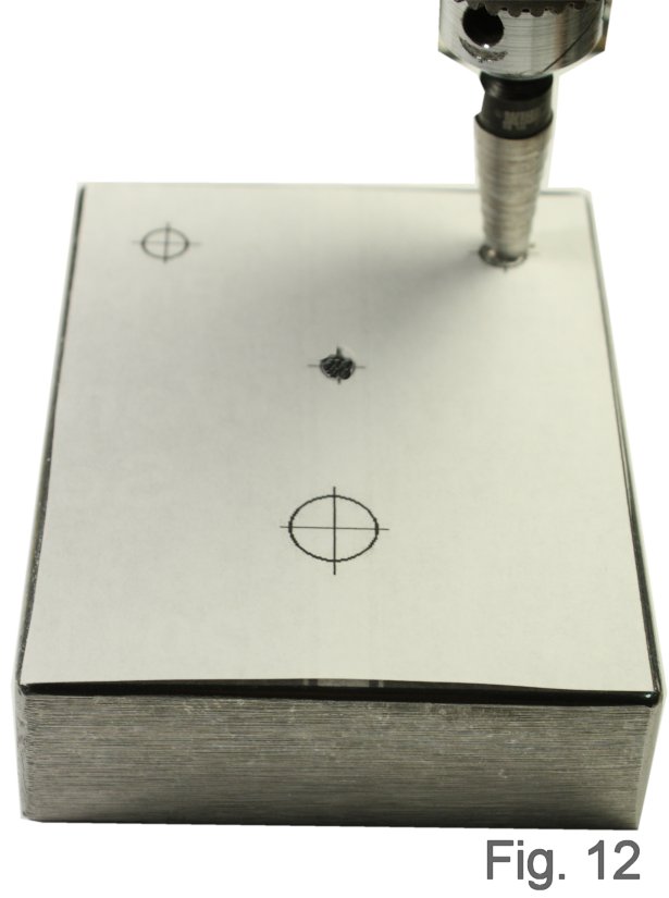
Many people like to use a step drill (the Irwin Unibit is a popular brand) because it does a quick, clean job of boring any size hole from 1/8" to 1/2" (Fig. 12). If necessary, de-burr all of the holes with a small, round file. Remove the templates and tape for the holes you have drilled.
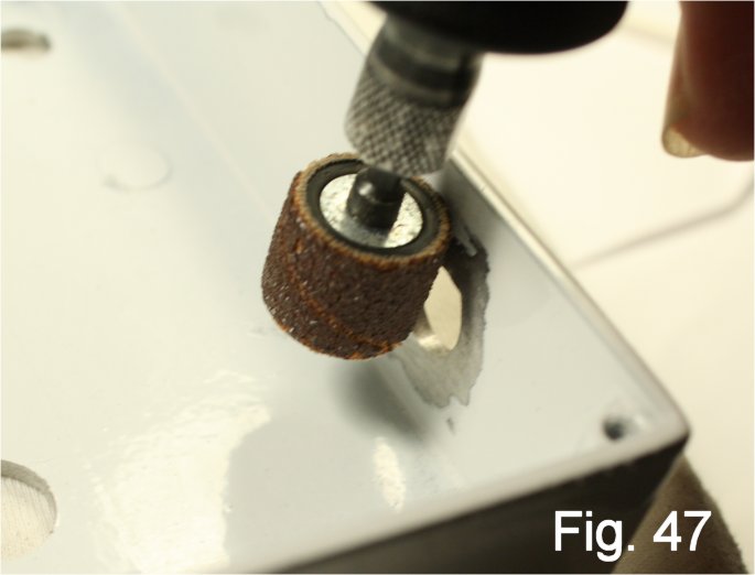
There will be molding artifacts on the inside that should be ground out so that all components have a flat purchase. A stone on a Dremel tool does this in seconds, or use sandpaper.
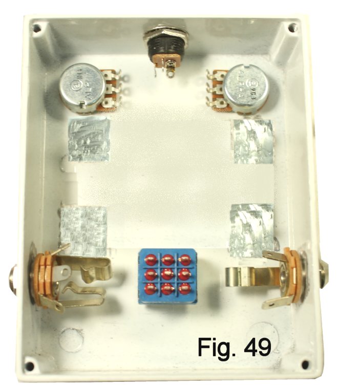
At this point, the tooling of the enclosure is finished and it is ready for painting and decorating. There are numerous "recipes" on-line for doing this.
Assembling The Board
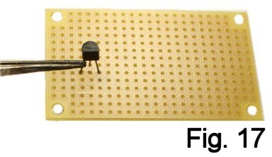
If you have built an effect on perfboard, like the Tweak-O, you will be familiar with this method of construction. If this is your first build, you may want to look at that article and possibly practice making connections on a scrap piece of material before you commit to this build.
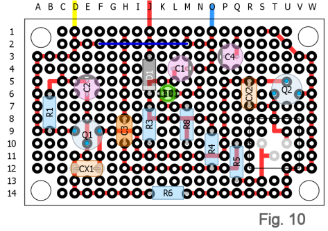
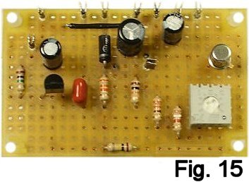
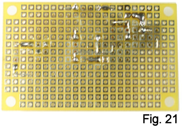
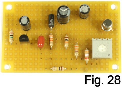
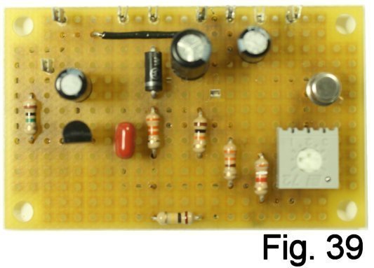
Figure 14 is a layout drawing and a parts list and figure 15 is a pic the top of the finished board. The layout shows the board in "X-Ray" view; the red lines are connections that we will make with bare wire on the bottom of the board. Print a copy of this drawing and the schematic so that you can mark off connections with a highlighter as you work. This is one of my proven methods for catching mistakes before they cost me time and frustration.
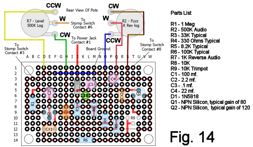
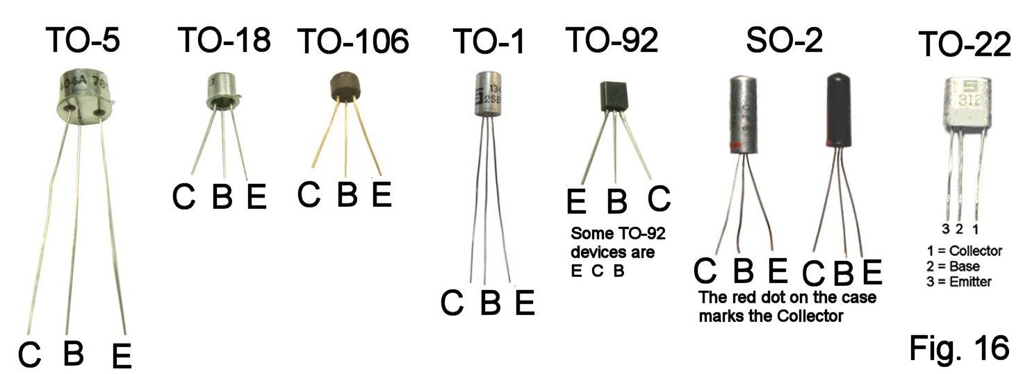
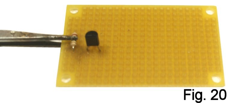
Identifying Transistor Pinouts
The layout drawing shows where Collector, Base and Emitter connect on the board, but where they are on the device will differ with the style of the transistor case. The board layout is for a TO-5 can, but other pinouts can be accommodated by bending their leads. Figure 16 shows some pinouts that you may encounter.
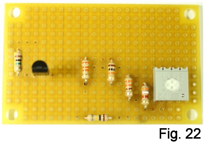
The board has room for bias trimpot R9, and it is shown in this build to indicate where it goes (Fig. 21 and Fig. 22). It is not needed if you know the correct value for resistor R5 from having tweaked the bias on the breadboard.
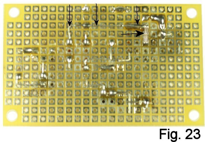
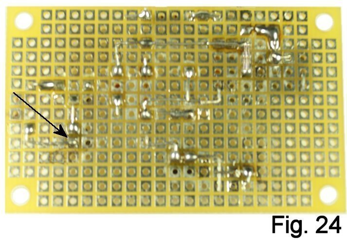
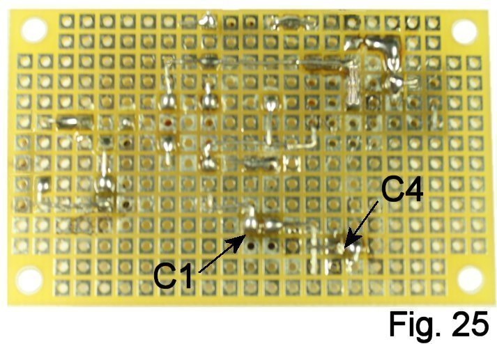
When adding the electrolytic capacitors, C1, C2 and C4, observe polarity! The negative side will have a stripe on it. The negative side of C2 is routed to connect to R1 and the positive side meets up with the Base of Q1 (Fig. 24).
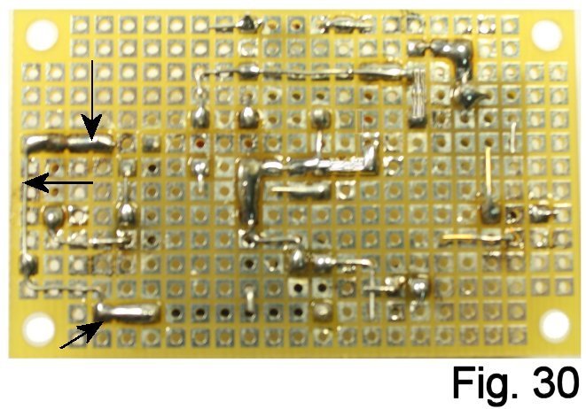
When planning a board layout for manufacture as a printed circuit board, jumpers are sometimes a way to avoid the expense of a double-sided PCB. The jumper on the component side is shown as a thin blue line in the layout drawing. While jumpers are often bare wire, I used insulated here to avoid any chance of a short to the pin of diode D1. Cut a piece of wire to span eight holes, install in indexes F-2 through M-2 and solder in place (Fig. 29).
On the bottom side, butt a short length of bare wire up to the end of the jumper at index F-2 and solder (Fig. 30). With the chain-nose plier, create a sharp right-angle bend at index D-2. (I'll show you later when we do terminations how to make the connection to the potentiometer at D-1.) "Tack" the run with a dab of solder at index D-2, and bend again at index D-3. Bend downward in column A. Hold the run in place with the tweezers and add solder to connect indices A-9 through D-9 (Fig. 30).
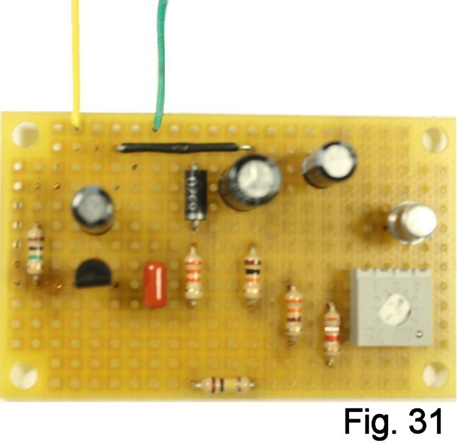
Many DIY builds will have you insert leads in the holes (Fig. 31), connect to pots, jacks and switches and then stuff the board in the enclosure. I find this method tacky and won't teach that way. One "right" way to terminate to an off-board component is to insert a push-in terminal (I call these "flea clips") into the appropriate hole and solder on the underside of of the board. Then you can mount the board on standoffs and wire to the terminals.
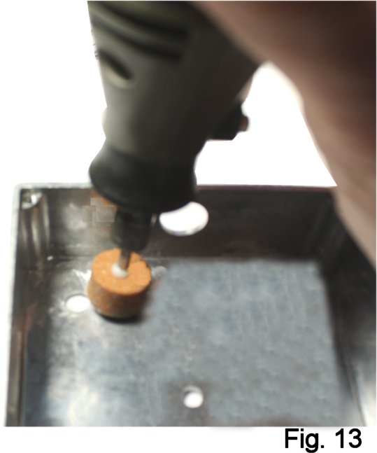
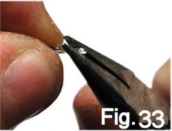
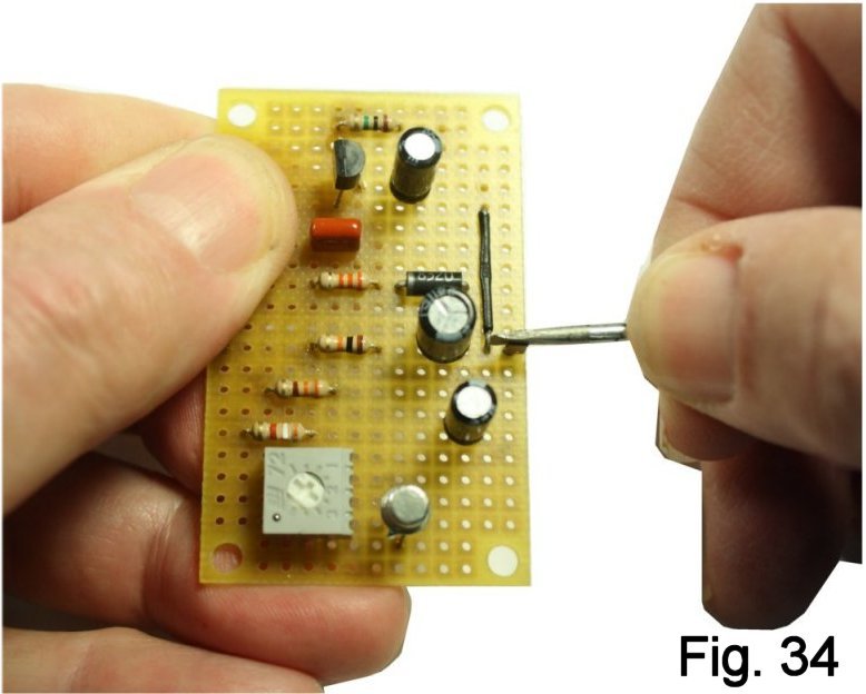
Start with the hole at index M-1. Enlarge the hole slightly by "working" it with an awl or straight pick (Fig. 32). Squeeze the bottom of the terminal slightly with the chain-nose plier (Fig. 33), insert in the hole, and push down in the top slot--firmly and steadily--with the side of a small screwdriver to seat the terminal. Heating the terminal while pressing it in with a soldering iron also helps. (Fig. 34).
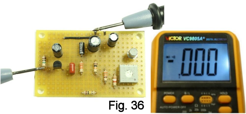
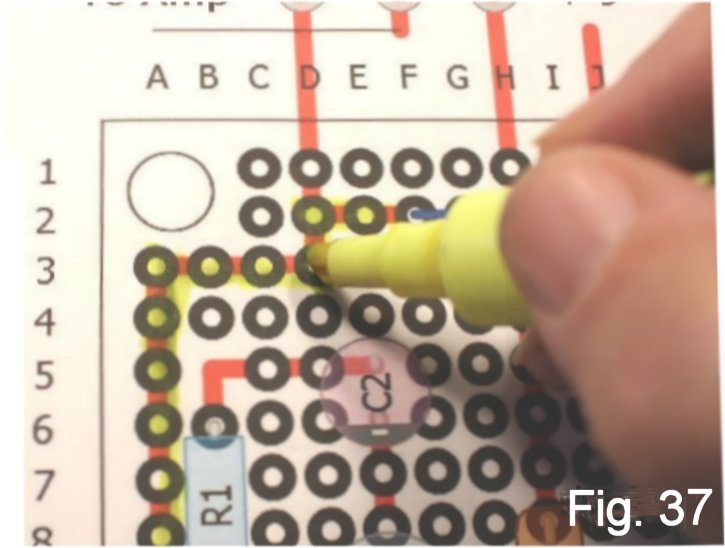
Now you can do a continuity test from the terminal at index O-1, to M-1, back to one side of R1 and the Emitter of Q-1 (Fig. 36). As you test connections, mark them off with a highlighter (Fig. 37).
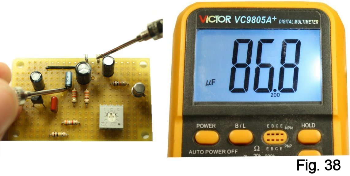
If your multimeter has a capacitance scale (as many do), it's possible to test continuity through a section that contains a capacitor.
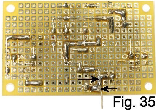
Look at the layout drawing again. The negative (bar) side of diode D1 sees the + side of capacitor C1 as well as resistors R3, R8 and R4. This is the positive supply bus. I started this run at the + side of C1 (index L-4), bent toward the diode and then downward to J-6. I soldered there and then continued to connect the resistors.
We have also already made the connection between the negative side of C1 and the ground bus. So it would make sense that if we measure capacitance from the negative (bar) side of D1 to any point on the ground bus, we should see about 100 mf. (Fig. 38). The meter shoes 86.8 here, and that's within the normal 20% tolerance for an electrolytic, so we are good. You should see the same reading from the sides of R3, R8 and R4 that connect to the positive supply bus. Use this technique wherever convenient to help ensure correct wiring!
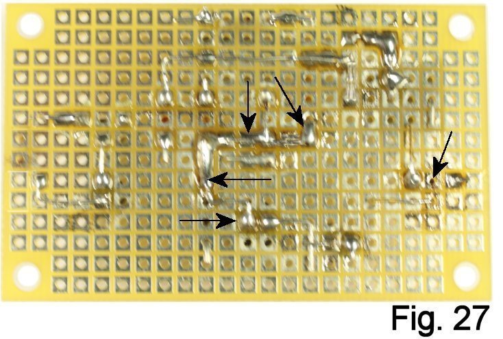
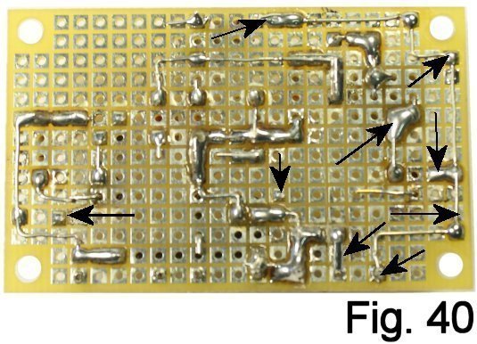
- Collector of Q2 to the trimpot (Fig. 40)
- Terminal at S-1 to Emitter of Q2. Then continue to resistor R6 (Fig. 40)
- Insert a bare lead into the hole of the flea clip at index Q-1. Solder there and at the positive side of capacitor C4 (Fig. 40).
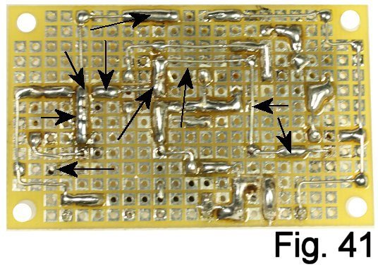
- Butt a bare lead to index S-5 (near the Base of Q2) and solder. Bend down in column P and across in row 11. Cut off at index I-11 and solder to join resistor R3. Finish the run to join the Collector of Q1 (Fig. 41).
- Make the connection from R6 to the Base of Q1 (Fig. 41).
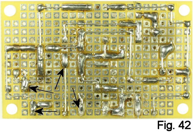
- Insert a bare lead in the hole of the terminal at H-1, route to capacitor C3 and solder (Fig. 42).
- Insert a bare lead in the hole of the terminal at J-1 and solder to Diode D1 (Fig. 42).
- Insert a bare lead in the hole of the terminal at C-4 and solder to Capacitor C2 (Fig. 42).
- Insert a bare lead in the hole of the terminal at D-1 and solder to the ground line (Fig. 42).
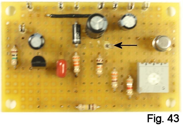
- Insert a flea clip at index N-6 with its flanges at right angles to all the others (Fig. 43).
The wiring is done. At this point, I suggest printing out a copy of the schematic and the layout and doing a thorough point-to-point continuity test. If everything is correct, assembly begins with installing the in-use LED.
Assembly
Keep in mind that you are now at a delicate stage, because you have put a lot of work into finishing the case. Slips, falls and mistakes with tools can ruin the finish and cost you a lot of grief, so stay focused and work patiently. Set yourself up with a towel or soft cloth on your bench to protect the face of the enclosure while you work.
I chose not to use a bezel for the LED; if you want one, this is the time to add it. Enlarge the hole as necessary with a reamer.
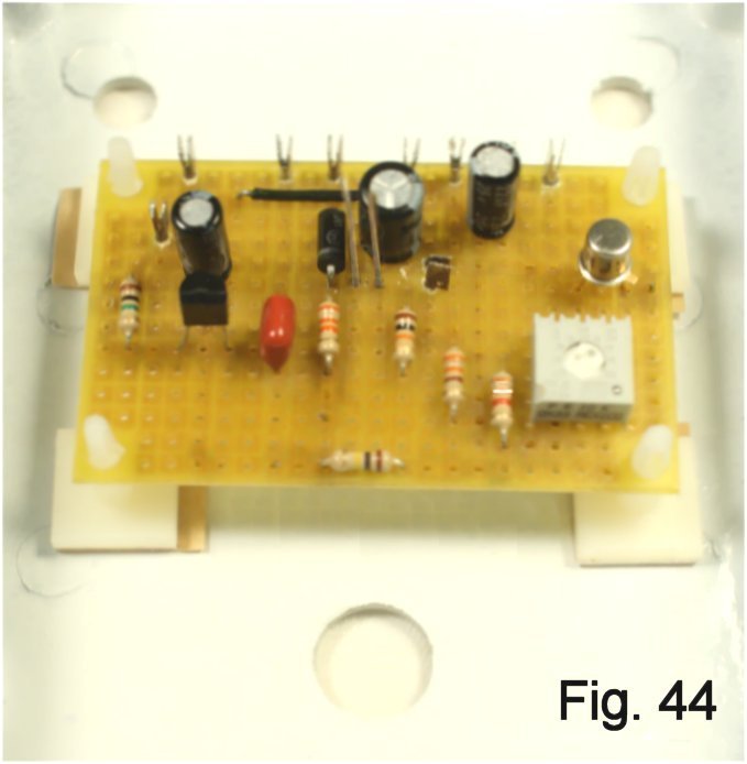
Insert a plastic standoff into each mounting hole of the board, but do not remove the paper backing from the adhesive yet. Slip the LED into its holes on the board; the longer (positive) lead goes in index K-6, and the short (negative) lead goes in index L-6. Set the board in place in the enclosure, making sure that the LED is straight up-and-down and the board is centered and parallel with the holes for the pots and switch (Fig. 44).
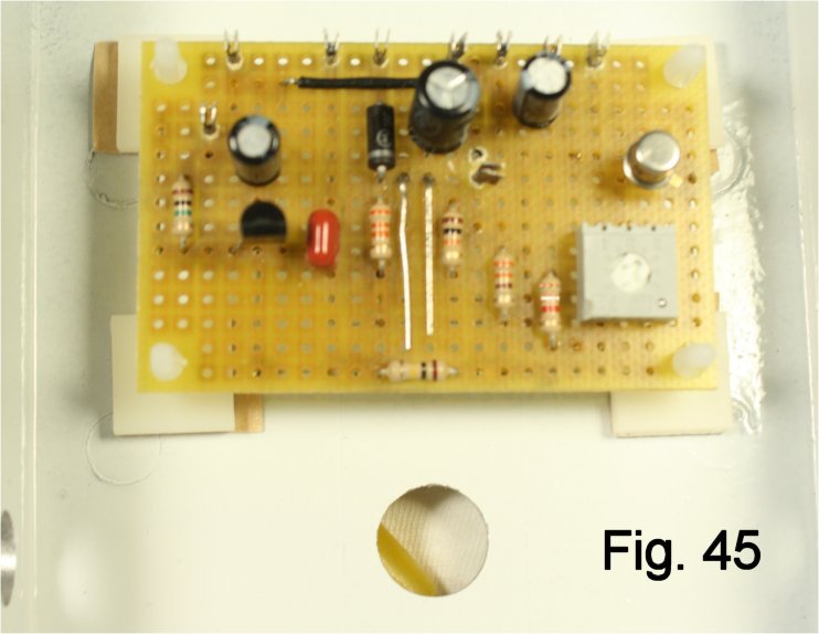
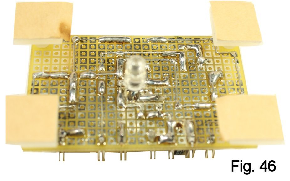
Making sure that the LED is fully inserted in its hole, bend its leads sharply toward the surface of the board (Fig, 45). This sets its height. Hold in place with locking tweezers and solder in place on the bottom; connect the positive side to R8 and insert a bare lead in the hole of the flea clip at N-6 to connect to the negative side. The wiring is a little tight here, so inspect carefully and test for both continuity and shorts to other runs when you are done (Fig. 46). Slip the LED back into its hole and be sure that it seats itself, and the board, correctly.
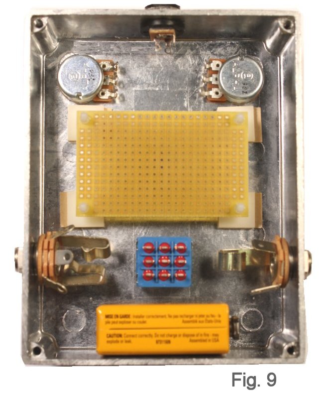
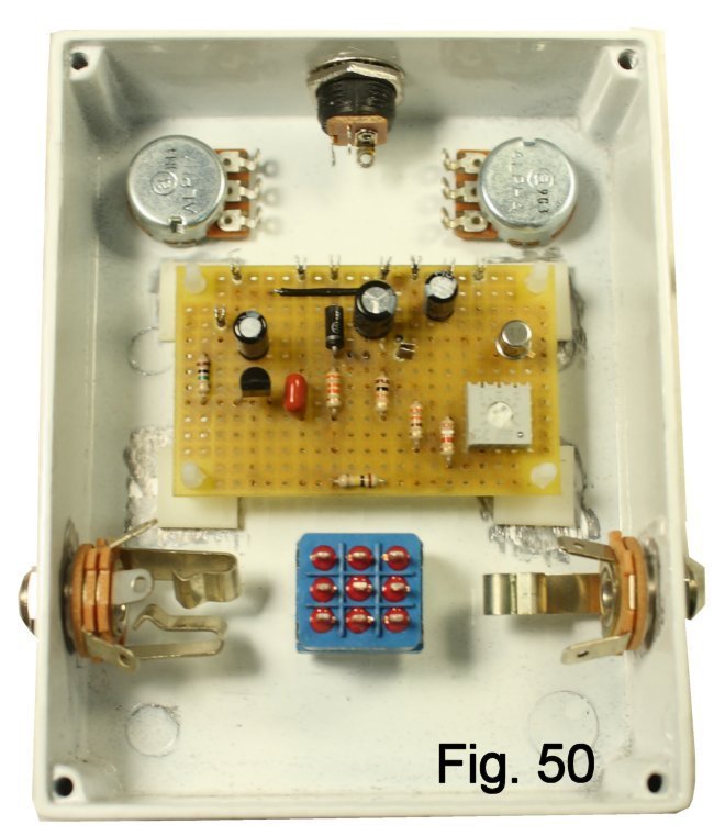
Remove the backing paper from the standoffs and carefully set the board in place (Fig. 50). I suggest not pressing it all the way in until you have finished wiring and testing.
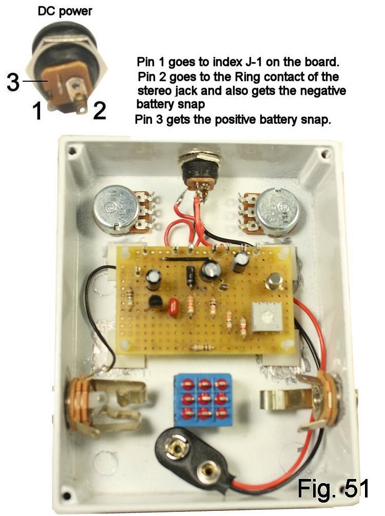
- Start with the power jack: Wire from the center-pin contact (#2) of the power jack to the Ring contact of the stereo jack. The center-pin also gets the negative lead of the battery snap. The positive battery snap lead goes to the switched contact, #3. Wire pin 1 to index J-1 on the board (Fig. 51).
- Create a ground run. From the board ground at M-1, wire to the sleeve of the stereo jack. From the sleeve of the stereo jack, wire to the sleeve of the mono jack. End the run at the stomp switch contact #9 (Fig. 52).
- CCW (Counter-clockwise) of the Level pot to the terminal at index D-1.
- W (Wiper) of the Level pot to contact #6 of the stomp switch.
- CW (Clockwise) of the Level pot to the terminal at index H-1.
- CCW (Counter-clockwise) of the Fuzz pot to the terminal at index O-1.
- W (Wiper) of the Fuzz pot to the terminal at index Q-1.
- CW (Clockwise) of the Fuzz pot to the terminal at index S-1.
With this much done, connect a battery and stick a guitar plug in the input so that the board is powered. The trimpot, if you built with it, should be about at its midpoint. Measure the voltages at Collector, Base and Emitter of both transistors and compare with this table.
| Collector | Base | Emitter | |
| Q1 | 1.56 | .65 | 0 |
| Q2 | 4.93 | 1.56 | .93 |
Try various settings of the trimpot. YMMV depending on transistor gains and the trimpot setting, but any serious differences or inability to adjust are a sure indication that something is not wired right. Keep in mind that hand-wired boards are by nature more subject than printed circuit boards to problems with continuity and and shorts. Check everything against the layout and the pics. This being essentially a Fuzz Face, there are gazillions out there who have built it and can help you debug. The Forum at diystompboxes.com is an amazing resource for this.
Final Assembly
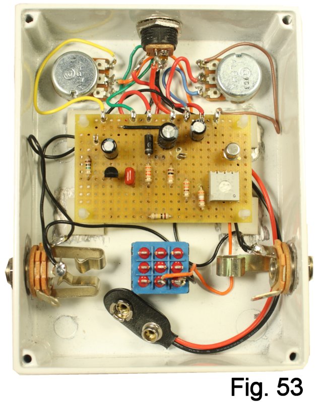
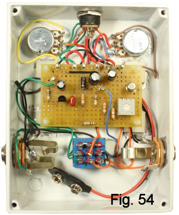
Complete the wiring of the stomp switch (Fig. 54).
-
Connect contact #1 and contact #4 with a bare-wire jumper.
-
Connect contact #2 to the stereo jack Tip.
-
Connect contact #5 to the mono jack Tip.
-
Connect contact #3 to the terminal at index C-4.
-
Connect contact #8 to the terminal at index S-3.
Setup and Initial Testing
Connect your guitar and an amplifier and connect a battery. Try out the controls. If it sounds like a Fuzz Face, good job! Before you continue, connect a power supply and make sure that everything still works with/without a battery.
Now connect up your gear again and give the pedal a thorough test. Sound Hendrix-y enough for ya?
CONGRATULATIONS!
Tighten up the hardware and add knobs. Install some padding for the battery and add rubber feet.
Now for the FAQ that you were wondering if I would address:
Can I Use Germanium Devices?
Sure, with a couple of caveats. First, I purposely did this design with cheap, readily available NPN silicon devices so that anyone could build it and it would play gracefully on a board with other negative-ground pedals. No separate power supply is required. NPN germanium is available, but a pair that hits reasonable gain buckets and is not too leaky may cost you as much as all of the rest of the parts combined. It's not a conspiracy; for historical reasons, good quality NPN germanium is relatively scarce. See my stock list if you are interested. If you troll E-Bay, get some assurance from the seller that you will be able to return unsoldered devices that are hissy or excessively leaky.
The other thing I would suggest is using socket-pin material for all four bias resistors. Germanium varies so much in gain and leakage, and is so temperature-sensitive, that you may need more control than just adjusting one resistor will give you.
What If I Only Have PNP Germanium Devices?
The information here is still usable, but all polarities have to be reversed--power, diode and electrolytic capacitors. If I can make time for it, I'll do drawings for this version.
I hope you enjoy your new noise-toy. Comments and questions welcome at smallbearelec@ix.netcom.com.