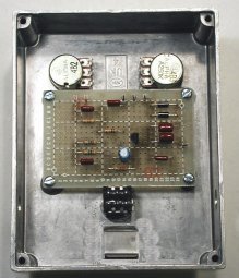
Tools and Materials
You'll need a 25- to 35-watt soldering iron, rosin-core solder and cleaning sponge and some other basics:
- Small screwdriver(s)
- Small diagonal pliers and cutters
- Small locking-grip ("Vise-grip") plier
- X-acto knife
- Self-locking tweezers or other "third hand"
- Small alligator clip
- Colored pencil or "Hi-liter" felt-tip marker
- Electric drill and twist drills from 1/16" to ¼" (a Dremel tool is also very helpful)
- Tapered reamer
- Some small round and flat files
- A pointed steel "pick" or scratch awl
- De-soldering braid (Radio Shack p/n 64-2090B)
- Mixing cup, stirrer and brush for epoxy sealer
For finishing the case you'll need:
- 220-grit and 400- (or finer) grit carborundum paper
- Acetone, denatured alcohol
- Spray primer and enamel
- Clear adhesive label stock
- Quick-setting epoxy glue
- Epoxy sealer
Check Out The Schematic
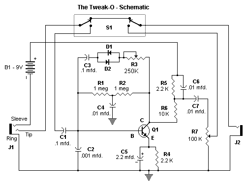
You don't have to understand or be able to interpret a schematic in order to build the Tweak-O. But its a good idea to at least take a look, so I'll give you a running start on the learning curve. The references at the end of this article will take you further. See figure 2.

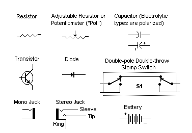
A schematic may look like an abstract painting, but well-drawn ones have a consistent logic once you learn what the symbols mean. Every symbol represents a component, and the symbols are internationally recognized; the symbol for a resistor is the same in the U.S. as it is in the smallest factory in the Far East. The straight lines represent component leads or connections between components, and the heavy dots indicate where component leads join. Only a few component types are used in the Tweak-O. See figure 3:

The symbol 
means "ground" or "common". In this case, ground does not mean a connection to the Earth itself; it just means that all the points that show this symbol are connected together. Ground is the point from which all voltages are measured.
Every component type has a designating letter, and individual components are numbered for identification; so, resistors are always "R" and capacitors are always "C", for example. Transistors are always "Q". This system makes it easy to locate, for example, "the junction of the emitter ("E") of Q1, the positive side of C5, and R4."
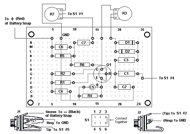
A schematic shows the logical relationships between components, but it doesn't necessarily show physical relationships--where components are mounted in relation to each other. Once a circuit has been proven to work, a designer's first job is to translate the schematic to a suitable layout on a chassis or circuit board. I have done this, and the layout in figure 4 is the drawing from which we will build.

This layout drawing is about 1 1/2 times actual size. Because I'm teaching, I made it larger than I usually would. Also, I was more than usually generous with space between components. But in all other respects, it represents the way a professional might wire a prototype. The drawing shows outline views of the components in heavy lines, and it shows how they connect to each other in gray lines. The connecting lines are in "X-Ray" view; that's to say that you are seeing directly the components on the top of a circuit board, and seeing the connecting wires through the board. If this isn't clear right now, it will be when we start to wire.
At this point, you might want to start getting familiar with the components you've bought by matching and looking at them against both the schematic symbols and the layout drawing. The references at the end will give you more information about recognizing components and reading values and color codes. You can also E-mail me with specific questions.
Construction Methods - Using Perfboard
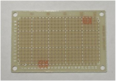
Perforated circuit board, or perfboard as it is commonly called, is a convenient material for building a hand-wired prototype. Component leads are inserted through the holes in the board and soldered in place on the opposite side. Connections are made with short lengths of bare wire. The kit comes with a custom-made perfboard that has pre-drilled holes. Each hole has a tinned copper pad to which solder can bond. This type of stock is called, appropriately, pad-per-hole perfboard. If you are buying parts locally, Radio Shack offers a piece of pad-per-hole, p/n 276-149, that is the same size. Both sides of your board are indexed; if you look at figure 5, you'll see that every one of the 356 holes in the board can be identified by a letter-and-number coordinate. I use the indexing on the board to refer to the position of every joint in the layout drawing. You can locate the components and do the wiring "by the numbers". Are you ready to build? Let's go!

Before we mount components on the board, we have to tool the case and locate the places where we will later attach mounting studs. This is actually harder than building the board, but its the most fun once you learn the techniques involved.
The commonest type of enclosure for effects is a cast aluminum box with a screw-on lid. The Hammond model 1590-BB was a standard for many years, but less expensive clones have recently become very popular. The one that comes with with the kit is made by Eddystone, Hammonds European subsidiary.
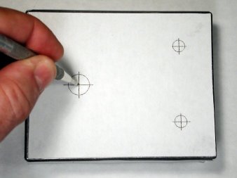
The most important step in tooling your box is locating the holes for switch, controls and jacks such that these components will fit in and around the board. Its very frustrating to be putting an effect together and finding that a jack is trying to occupy the same physical space as a capacitor. Fortunately for you, Ive done all of the planning. If you use the enclosure in the kit and these drilling templates, youll find that the Tweak-O goes together just like a jigsaw puzzle. Take a look at figure 6.
Remove the four screws that secure the lid to the enlosure. With a good, sharp scissor, cut out the top template. Attach a couple of pieces of double-sided clear or masking tape to the box, and carefully center the template to the cover. In the same way, attach the templates for the sides, being careful to get the holes for the jacks in the correct locations to the right and left of the switch. Now use a scribe or scratch-awl to put a small dent at the center mark of the hole for the stomp switch.

Notes On Drilling The Holes: Many people have started using the Irwin Tool Unibit rather than separate drills, because it does a quick, clean job of boring any size hole from 1/8" to 1/2".
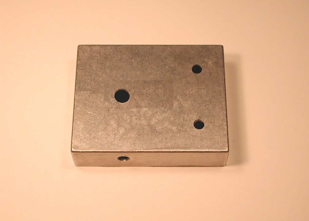
If you use standard twist drills, bore a 1/8" pilot hole, enlarge it with a ¼" drill, and then use a tapered reamer to slowly bring the hole to its final size. Follow the same procedure for the other two holes on the top, and then the holes on the sides. De-burr all of the holes with a small, round file. Remove all of the templates and tape, and you should have the result shown in figure 8.


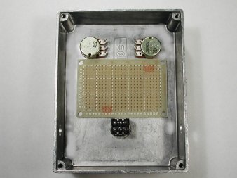
The next step is to mount the switch and the pots temporarily, and use the perfboard itself as a guide to make sure that the holes are properly positioned. See figure 9. If you have done the drilling correctly, the board should just fit between the switch body and the pots.

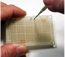
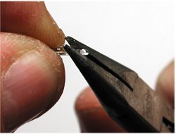
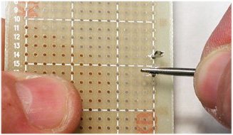
We are ready to populate the board. Your first job is to install six push-in terminals that will be used later as tie points for connections to the pots, jacks and stomp switch. Referring to the layout drawing, these go at O-5, O-7, O-14, O-16, O-18 and F-25. Enlarge each hole by "working" it slightly with an awl or steel pick before you try to insert a terminal (figure 10). I have found that the terminals go in more easily if you squeeze the bottom just a little with diagonal pliers (figure 11) and then push down firmly but gently in the top slot with the edge of a small screwdriver (figure 12).


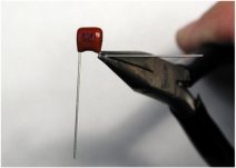
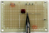
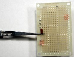
The first component we will solder in place is capacitor C7 (.01 mfd., marked 103J), which goes between points N-10 and N-14. Using diagonal pliers, bend each lead of the capacitor outward as shown in figure 13. Then put a right-angle bend in each lead so that the capacitor will span the five holes when inserted. To aid in locating the bends, put the component flat on the board and use the the holes as a guide as shown in figure 14. Insert the capacitor in place and secure one side with a pair of locking tweezers as in figure 15.


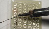
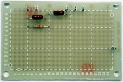
Solder one side in place, using as little solder as needed to fill the pad. Remove your "third hand", and clip the lead. (If you did not buy the kit, save those scraps of bare wire for use in making connections! I provide bare tinned wire as part of the kit.) Solder the other side and trim as in figure 16. In the same way, add capacitor C6 (also .01 mfd.) between points M-5 and M-9, and resistor R5 (4.7K, Yellow/Violet/Red) between K-5 and K-10. I sized the bends in all the resistors to span six holes to keep the layout wide and easy to work with. Thus far, things should look like figure 17.


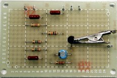
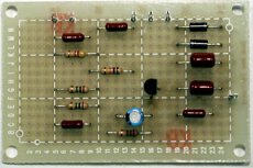
Keep adding components, working left to right. Note that the electrolytic capacitor, C5, is polarized; the negative side has a black band running down the body. Also note the band marking the polarity of the diodes, D1 and D2. While silicon transistors and diodes are not as heat-sensitive as their germanium counterparts, it is a good idea to use an alligator clip as a heat sink, putting it on each lead of the device before soldering as in figure 18. Figure 19 shows the board fully populated.


For reference, here's a table of component positions:
|
Component |
From |
To |
| C6 |
M-5 |
M-9 |
| R5 |
K-5 |
K-10 |
| R2 |
G-5 |
G-10 |
| R1 |
E-5 |
E-10 |
| C4 |
C-5 |
C-9 |
| C7 |
N-10 |
N-14 |
| R6 |
I-9 |
I-14 |
| C5 |
D-12 |
D-16 |
| R4 |
B-11 |
B-16 |
| Q1 Collector |
H-16 |
|
| Q1 Base |
G-17 |
|
| Q1 Emitter |
F-16 |
|
| D1 |
N-19 |
N-24 |
| D2 |
L-19 |
L-24 |
| C3 |
J-19 |
J-24 |
| C1 |
G-19 |
G-24 |
| C2 |
D-19 |
D-23 |
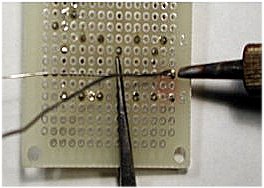
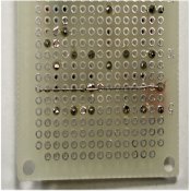
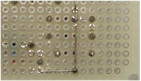
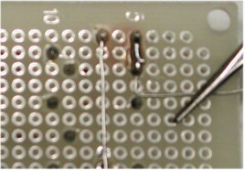
With all the components in place, we begin to make connections between them with short lengths of bare tinned wire. First we'll do a long one: the beginning of the ground line that starts at point O-7. As shown in figure 20, butt a length of bare up to point O-7. Use the locking tweezers to hold it in place and add solder at O-7. To make it mechanically stable, "tack" this lead by soldering at point G-7. Then you can cut the lead off at point A-7. So far, things look like figure 21.
Now butt a short length of wire to the end of the lead at point A-7. Hold it down with the tweezers and solder. Cut it off past point A-11, leaving just enough at the end to bend upward toward point B-11. This is shown in figure 22.


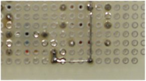
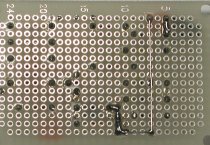
Using diagonal pliers, bend the lead up toward point B-11. Trim the end if necessary so that it just butts against the existing solder joint, and add solder. See figure 23 and figure 24. Finish this run by butting a lead to point B-11 and soldering. Cut the free end, leaving a very short length to bend toward point D-12. Make this bend and solder. The completed run is shown in figure 25.


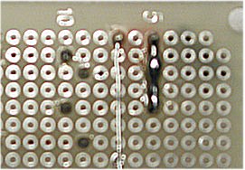
If you are with me so far, you have the basics of the technique. Where you need to bridge only a short span, put a right angle bend in the end of your bare wire and use the tweezers to hold it in the gap. Fill the gap with solder and clip the bare wire away right at the joint. I did this to join points O-5 and M-5, and then I did it again to join M-5 and K-5. You can see the progress and the results in figures 26 and 27.


Here is a table of the rest of the connections in the order I did them, with some notes where appropriate.
It's a good idea to mark off connections on the layout with a highlighter as you
do them.
| A-11 to A-23 |
Tack at A-17 |
| A-23 to D-23 |
|
| C-9 to A-9 |
I used the flat of an X-acto knife to lift the
ground run slightly and slip a bare lead through to butt against C-9.
Solder and clip. |
| G-5 to E-5 to C-5 |
|
| F-16 to D-16 to B-16 |
|
| G-10 to H-16 |
Solder an end to G-10 first. Use pliers to
right-angle bend the wire in row 12. Then bend it again toward H-16. Trim,
solder and tack at the bend. |
| H-16 to O-16 |
|
| I-14 to I-16 |
|
| E-10 to G-17 |
This is another connection that is best done
using two right-angle bends. |
| N-10 to K-10 to I-9 |
Do a very short right-angle bend to finish at
I-9. |
| N-14 to O-14 |
|
| M-9 and M-10 |
Flow solder between the points to make this
connection. |
| J-19 to G-19 to D-19 |
|
| G-17 to G-19 |
|
| A-23 to E-23 |
|
| J-24 to L-24 to N-24 |
|
| J-19 to L-19 to N-19 to O-18 |
|
| G-24 to F-25 |
|
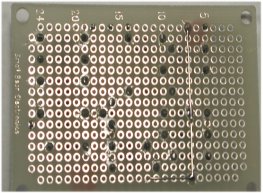
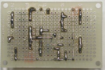
The board is done! Figure 28 is a pic of the finished solder side.

I know that you are hot-to-trot to try it out, but this is really the best time to paint and decorate the case.
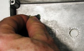
Once you have the case finished to your liking, you can install the pots, switch and jacks and mount the circuit board. Remember that we marked earlier the positions for the mounting studs for the board? Go over these points with fine sandpaper now and clean up with alcohol or acetone. See figure 29.
Install the pots and the stomp switch, being careful not to touch the areas that you just cleaned up. Install a screw in each corner of the board, and screw on a stud finger-tight. Just as you prepared the mounting surfaces, sand the sides of each stud and clean with solvent as in figure 30.


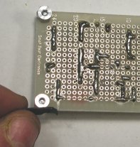
Mix some quick-setting epoxy cement. Apply a small amount to the sides and bottom of each stud, and carefully lower the board into place as shown in figure 31. Give the adhesive a couple of hours to cure thoroughly. Carefully remove the screws, lift out the board, and add some more epoxy around each stud. When the adhesive has cured fully, re-install the board. The battery clip is mounted below the stomp switch in the same way that you installed the studs: sand both surfaces, clean up with solvent and secure with epoxy cement. When the adhesive has cured, install the jacks. You are ready to wire to the off-board components!

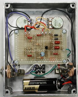
Here is a pic of the fully wired pedal. You have some leeway about how you route the wires, though I suggest keeping them out of the way of the contacts of the jacks. Three wires terminate at the ground pin O-7. I suggest putting all three in place first, and then soldering.

Make the connections as shown in the layout drawing. Pay close attention to getting the connections correct to J1 and J2. Note that the drawings show the Switchcraft jacks that come with the kit; if you are using some other make, the contact arrangement may differ.
As you did when wiring the components on the board, I suggest marking off these
connections with a highlighter as you make them. For reference, here is a list:
| Ring of J1, Ring of J2 and "Cold" side of pot R7 to O-7 (GND) |
| "Hot" side of pot R7 to O-14 |
| Red lead of battery snap to O-5 |
| "Wiper" of pot R7 to stomp switch contact #1 |
| "Cold" side of pot R3 to O-16 |
| Wiper and "Hot" side of pot R3 to O-18 |
| Black lead of battery snap to J1 sleeve |
| J1 tip to stomp switch contact #5 |
| J2 tip to stomp switch contact #2 |
| F-25 to stomp switch contact #4 |
Yep, we are finally ready to try it out! Connect your guitar and amp, and set both controls to mid-range. If you don't hear fuzz, click the stomp switch. Got the effect? CONGRATULATIONS! You can button up the case and attach the self-stick rubber feet to the bottom.
It Doesn't (*&%$?":!! Work!
First, take a shower and grab a bite, since we know that you haven't done either one since you started this thing; troubleshooting requires a clear head and normal blood-sugar level. The first rule thing to keep in mind is that projects like this are all-or-nothing. If EVERYTHING is correct, the pedal works; if ONE thing is wrong, it doesn't. But you have something going for you: The drawings have been vetted by a bunch of other builders, and you can rely on them. Use them as your bible, and you'll find out what's wrong.
I would start troubleshooting by making clean copies of both the schematic and the layout drawing. Use a highlighter to mark off connections as you check them. Go over the off-board connections first. If those look good, you have to verify the interconnections. If you don't have a multimeter, the only way to do this is to remove the screws holding the board, remove the retaining nuts from the controls, and gently lift the whole works free. Turn the assembly to the solder side and check your work. If you have a multimeter, you can do a lot without lifting the board: Use the continuity setting to make sure that you actually have a connection between every point in the layout that is supposed to be connected. Found a bug? Time to do repairs.
You can also use the low-voltage scale of your meter to sniff out problems. Hang the negative lead on point O-7. With both controls at mid-range, you should see roughly the following voltages on Q1: Collector 2.8 volts, Base 1.5 volts, Emitter .95 volts. If any of your readings are off these by more than 10%, you probably have a wiring error.
Its Great, But Id Like It To Sound More
There are MANY changes that you can try, but its best to do this kind of experimenting on a prototype breadboard. Buy another set of components (costs beans because you dont need the box or the switch) and you can fiddle to your hearts content. Try different capacitor values and different diodes; in particular, using germanium diodes instead of silicons produces a different effect. Another thing to try is removing the diode loop from the circuit entirely and seeing how you like the Tweak-O as a flat boost. Yes, you can put a simple switch in the diode loop so that you can switch between flat boost and distortion. A footswitch for this? Certainly, but you might want to plan a new layout that leaves enough room for a second stomp switch. Are you getting the itch to try another pedal? Careful, theyre like peanuts!
Parts List/Bill Of Materials For The Tweak-O
|
Reference or Quantity |
Description |
Mouser p/n |
Radio Shack p/n |
|
|
Fixed resistors are ¼ watt, 5% tolerance, carbon film or composition. Pots in the standard build are 16mm diameter; see the notes if you must use 24mm. Linear taper potentiometers will work, but the controls will "feel" funny. |
|
|
|
R1, R2 |
1 megohm |
291-1M |
271-1356 |
|
R3 |
250K audio taper potentiometer |
313-1000-250K |
|
|
R4 |
2.2K |
271-1325 |
291-2.2K |
|
R5 |
4.7K (2.2K in the original, but this gives a hotter output) |
271-1325 |
291-2.2K |
|
R6 |
10K |
271-1335 |
291-10K |
|
R7 |
100K audio taper potentiometer |
313-1000-100K |
271-1722 |
|
C1, C3 |
.1 mfd. poly-film or mylar |
140-pf1h104K |
272-1069 |
|
C2 |
.001 mfd. poly-film or mylar |
140-pf1h102K |
|
|
C4, C6, C7 |
.01 mfd. poly-film or mylar |
140-pf1h103K |
272-1065 |
|
C5 |
2.2 mfd. (or 4.7 mfd.) 16 volt radial electrolytic |
140-XRL16V2.2 |
272-1024 |
|
D1, D2 |
1N4001 silicon diode |
625-1N4001 |
276-1101 |
|
Q1 |
2N5089 or similar NPN silicon transistor (2N3904 in the original) |
610-2N5089 |
276-1617 |
|
J1 |
1/4" Stereo Jack, Switchcraft #12B or similar |
274-312 |
502-12B |
|
J1 |
1/4" Mono Jack, Switchcraft #11 or similar |
274-252 |
502-11 |
|
S1 |
DPDT alternate-action switch |
107-SF12020-L |
|
|
B1 |
9 volt transistor radio battery |
|
|
|
B1 |
Cast-aluminum box, Hammond 1590BB or similar |
546-1590BB |
|
|
1 |
Pad-per-hole perfboard |
|
276-149 |
|
6 |
Push-in terminals |
574-T42-1/C |
|
|
2 |
Knobs for ¼" shaft |
5164-1510 |
274-415 |
|
4 |
4-40 x 1/4'" threaded spacers |
534-1891 |
|
|
4 |
4-40 x 1/4'" screws |
5721-440-1/4 |
64-3011 |
|
1 |
9-volt battery snap |
123-6008 |
270-325 |
|
1 |
9-volt battery clip |
534-080 |
270-326 |
|
4 |
Rubber Feet |
517-SJ-5023 |
64-2342 |
|
|
Tinned bare connecting wire |
602-299/1-100 |
278-1341 |
|
|
#22 or #24 stranded hookup wire |
602-3050-100-xx |
278-1224 |

