Breadboarding A Rangemaster
By Steve Daniels, Small Bear Electronics LLC
Revised and © 2016 By Small Bear Electronics LLC
| The Dallas Rangemaster has been one of the most popular DIY builds for decades, and deservedly so; its blend of treble emphasis and soft clipping is unique, and it's inexpensive and not hard to duplicate. | |||||||||||||||||||||||||||||||||||||||||||||||||||||||||||||||||||||||||||||||||||||||||||||||||||||||||||||
When Small Bear first started up, there was still a lot of mystery
surrounding the "right" transistor for the RM. Thanks to the work of many
people, especially R. G. Keen, we know more now. My own contribution has
been scouring basements for suitable raw stock and offering a wide choice of
devices that are pre-tested and guaranteed to work. In this article, I will show you how to set up
a Rangemaster on the breadboard and tweak
performance. Once you have set up something that you like, the components
can be turned into a gig-worthy pedal. You can build:
Later, I'll talk a bit about the details of these choices and why they matter. |
|||||||||||||||||||||||||||||||||||||||||||||||||||||||||||||||||||||||||||||||||||||||||||||||||||||||||||||
| If you have never used a solderless breadboard, please refer to the intro article on breadboarding before you continue. That How-To covers a lot of basic information and techniques; I presume that you have been through it, have done the demos, understand how the tool works and have started learning to use your multimeter. If you are already familiar with breadboarding, note that the level of detail in this article is meant to guide complete beginners, so please be a little patient. | |||||||||||||||||||||||||||||||||||||||||||||||||||||||||||||||||||||||||||||||||||||||||||||||||||||||||||||
| Figure 1 is the circuit for the Rangemaster using a single transistor. I'm showing it both PNP and NPN, so refer to the drawing that corresponds to the type of device that you have. The difference? Cost, more than anything else; at the time the Rangemaster first came out, NPN germanium was harder to make and more expensive than PNP. NPN devices remain more expensive today, but the resulting build is more pedalboard-friendly. | |||||||||||||||||||||||||||||||||||||||||||||||||||||||||||||||||||||||||||||||||||||||||||||||||||||||||||||
| |
|||||||||||||||||||||||||||||||||||||||||||||||||||||||||||||||||||||||||||||||||||||||||||||||||||||||||||||
|
|
|||||||||||||||||||||||||||||||||||||||||||||||||||||||||||||||||||||||||||||||||||||||||||||||||||||||||||||
| |
|||||||||||||||||||||||||||||||||||||||||||||||||||||||||||||||||||||||||||||||||||||||||||||||||||||||||||||
|
This is a more complex schem than the LED demo in the intro, but it's still less than a dozen parts. I have purposely not included jacks, stomp switch or power switching in order to keep it simple; we'll add those later. The only things to note right now are: |
|||||||||||||||||||||||||||||||||||||||||||||||||||||||||||||||||||||||||||||||||||||||||||||||||||||||||||||
|
|||||||||||||||||||||||||||||||||||||||||||||||||||||||||||||||||||||||||||||||||||||||||||||||||||||||||||||
| Before we start to build, here are answers to a few FAQs:
What's the disadvantage of the positive ground build? A: If you mix positive- and negative-ground pedals on your board, the positive-ground pedals Must either use batteries or have their own power supply. I have a PNP device, and I really want to build and run negative ground. Can I "turn the circuit upside down" to do that? A: It has been done, it sometimes works and sometimes oscillates badly. Not recommended.
I've heard that I can use a voltage converter IC to get a negative supply voltage? A: This can be done, but it's beyond the scope of this article. Get the PNP version working as shown here before you investigate this.
|
|||||||||||||||||||||||||||||||||||||||||||||||||||||||||||||||||||||||||||||||||||||||||||||||||||||||||||||
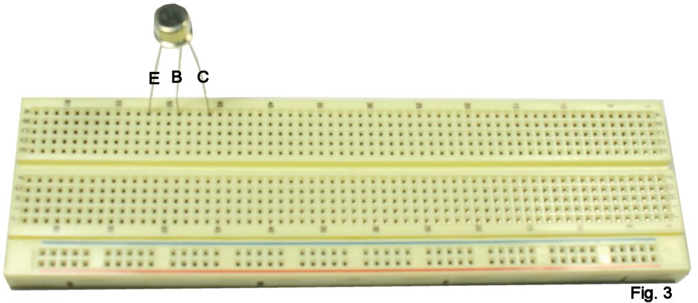
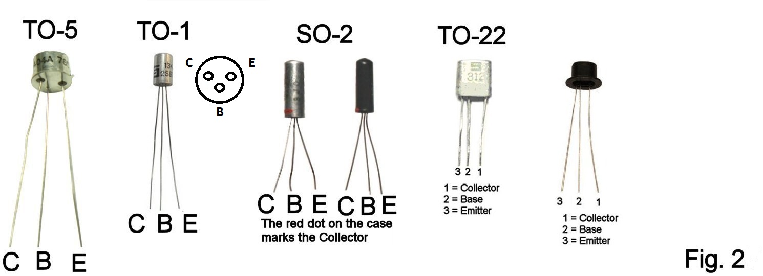
| Let's set up this circuit on the breadboard and try it out. The transistor you are using may come in one of many case styles, so compare it with Figure 2 and identify the Collector, Base and Emitter. Note that the case style is Not a guide to whether a device is PNP or NPN; you have to either know that based on the part number or supplier's description or determine it on a test instrument. | |||||||||||||||||||||||||||||||||||||||||||||||||||||||||||||||||||||||||||||||||||||||||||||||||||||||||||||
 |
|||||||||||||||||||||||||||||||||||||||||||||||||||||||||||||||||||||||||||||||||||||||||||||||||||||||||||||
| Now plug it into the breadboard. If this is your first build, you should follow my directions and layout this time around; once you have the idea, you're free to do whatever works. Similarly, I am working from left to right on the board, but that's not engraved in stone, either. For the sake of clarity, spread the leads out so that there are two holes between each lead. | |||||||||||||||||||||||||||||||||||||||||||||||||||||||||||||||||||||||||||||||||||||||||||||||||||||||||||||
|
|
|||||||||||||||||||||||||||||||||||||||||||||||||||||||||||||||||||||||||||||||||||||||||||||||||||||||||||||
| |
|||||||||||||||||||||||||||||||||||||||||||||||||||||||||||||||||||||||||||||||||||||||||||||||||||||||||||||
|
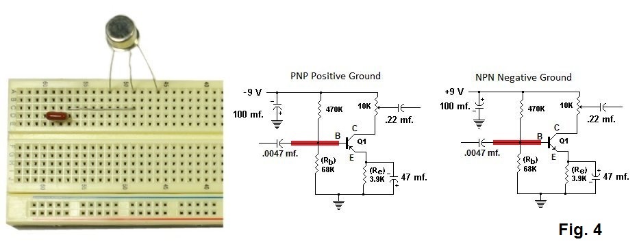
Cut and form a jumper to span 9 holes, and plug this in starting at the Base of the transistor. Find the .0047 mf. film capacitor (usually labelled 472J), trim its leads to 1/4" long and plug this in at the other end of the jumper. Figure 4 shows what you have done, both on the breadboard and in color in the schematics. |
|||||||||||||||||||||||||||||||||||||||||||||||||||||||||||||||||||||||||||||||||||||||||||||||||||||||||||||
| |
|||||||||||||||||||||||||||||||||||||||||||||||||||||||||||||||||||||||||||||||||||||||||||||||||||||||||||||
| |
|||||||||||||||||||||||||||||||||||||||||||||||||||||||||||||||||||||||||||||||||||||||||||||||||||||||||||||
 |
|||||||||||||||||||||||||||||||||||||||||||||||||||||||||||||||||||||||||||||||||||||||||||||||||||||||||||||
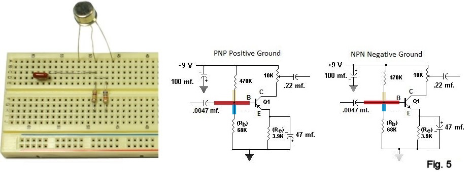
| Now we'll add the bias resistors for the Base. 470K is standard for all builds (Yellow, Violet, Yellow, Gold). The resistor noted as Rb is typically 68K (Blue, Gray, Orange, Gold). However, if you bought a tested device or a kit from me, it may be a different value to match the transistor. Find these two resistors, form leads to span six holes, clip to length and install as shown in Figure 5. Also add a very short jumper to connect the two resistors and the transistor Base. | |||||||||||||||||||||||||||||||||||||||||||||||||||||||||||||||||||||||||||||||||||||||||||||||||||||||||||||
 |
|||||||||||||||||||||||||||||||||||||||||||||||||||||||||||||||||||||||||||||||||||||||||||||||||||||||||||||
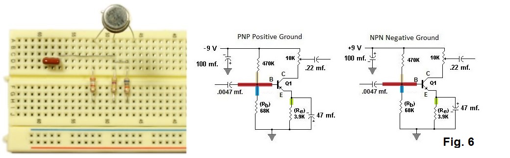
| Now add the Emitter resistor Re. This one is typically 3.9K (Orange, White, Red, Gold), but it, too, may be a different value if you bought a tested device or a kit. See Figure 6. | |||||||||||||||||||||||||||||||||||||||||||||||||||||||||||||||||||||||||||||||||||||||||||||||||||||||||||||
 |
|||||||||||||||||||||||||||||||||||||||||||||||||||||||||||||||||||||||||||||||||||||||||||||||||||||||||||||
| |
|||||||||||||||||||||||||||||||||||||||||||||||||||||||||||||||||||||||||||||||||||||||||||||||||||||||||||||
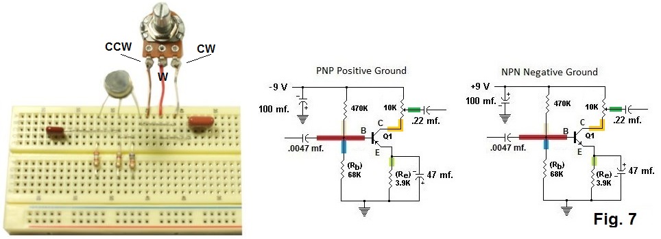
| Solder three short leads to the 10K audio taper (A10K) potentiometer and install as shown in Figure 7. Be sure to jumper as shown to the clockwise (CW) side of the control, or you'll wonder why it works "backwards" when you power up. You're also probably wondering why we have not made any connections to power or ground yet; I will walk you through those in a minute. Before we go there, add the .22 mf. (224J) output capacitor and the jumper that connects it to the wiper (W) of the potentiometer. This is a film capacitor, has no polarity and can be inserted either way. | |||||||||||||||||||||||||||||||||||||||||||||||||||||||||||||||||||||||||||||||||||||||||||||||||||||||||||||
 |
|||||||||||||||||||||||||||||||||||||||||||||||||||||||||||||||||||||||||||||||||||||||||||||||||||||||||||||
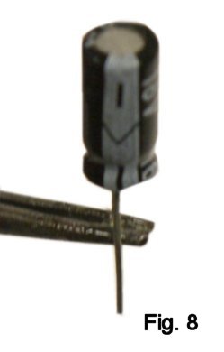
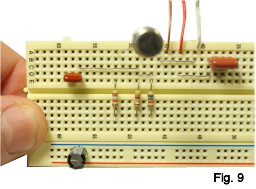
| The two electrolytic capacitors are both polarized. On radial-case types like this one, a band marks the negative side (Fig. 8). Trim the leads of the 100 mf. ("microfarad") electrolytic capacitor, following the convention of leaving 1/4" to 5/16" of lead length for insertion in the board. Plug it in to the power supply bus, positive side to positive rail and negative side to negative rail. I have tilted the breadboard so that this is clear (Fig. 9). | |||||||||||||||||||||||||||||||||||||||||||||||||||||||||||||||||||||||||||||||||||||||||||||||||||||||||||||
|
|
|||||||||||||||||||||||||||||||||||||||||||||||||||||||||||||||||||||||||||||||||||||||||||||||||||||||||||||
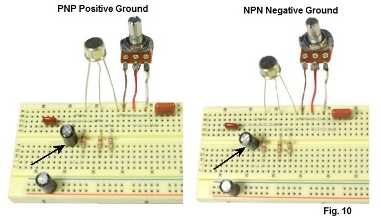
Form the leads of the 47 mf. electrolytic capacitor to span six holes.
Add short jumpers to connect the capacitor to the transistor Emitter and resistor Re. Figure 10 shows both orientations and the jumpers. |
|||||||||||||||||||||||||||||||||||||||||||||||||||||||||||||||||||||||||||||||||||||||||||||||||||||||||||||
|
|
|||||||||||||||||||||||||||||||||||||||||||||||||||||||||||||||||||||||||||||||||||||||||||||||||||||||||||||
| Now for the connections to the power rails.
If you are building PNP positive-ground:
|
If you are building NPN negative-ground:
|
||||||||||||||||||||||||||||||||||||||||||||||||||||||||||||||||||||||||||||||||||||||||||||||||||||||||||||
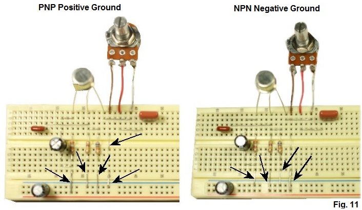
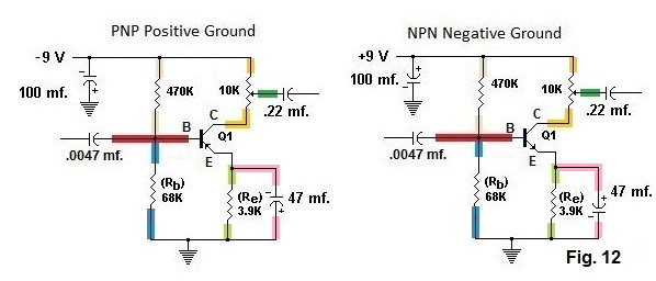
| Figure 11 shows the breadboard and figure 12 shows what has been done in the schematics. If this is your first build, take the time to compare the schems with the physical layout and be sure that you are clear about what connects to what and how. You might even pick up a mistake... | |||||||||||||||||||||||||||||||||||||||||||||||||||||||||||||||||||||||||||||||||||||||||||||||||||||||||||||
|
|
|||||||||||||||||||||||||||||||||||||||||||||||||||||||||||||||||||||||||||||||||||||||||||||||||||||||||||||
|
|
|||||||||||||||||||||||||||||||||||||||||||||||||||||||||||||||||||||||||||||||||||||||||||||||||||||||||||||
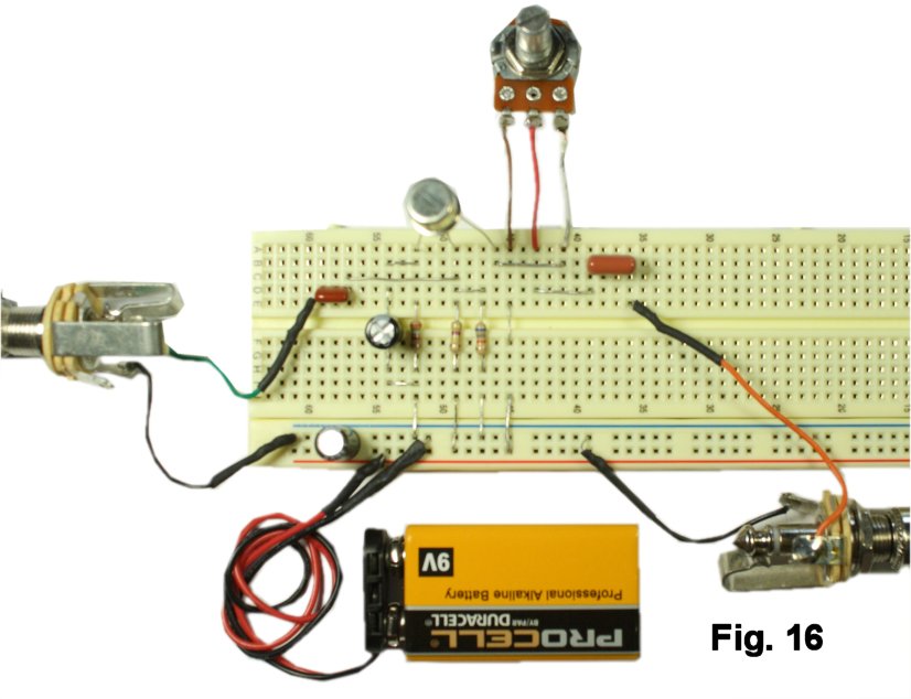
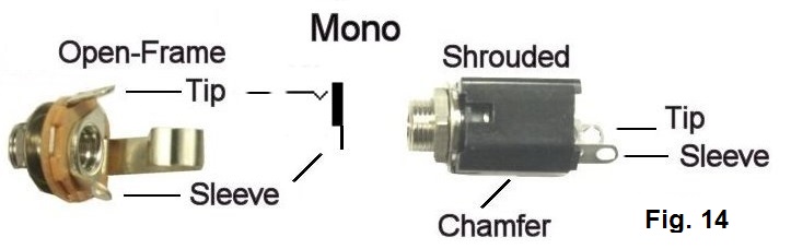
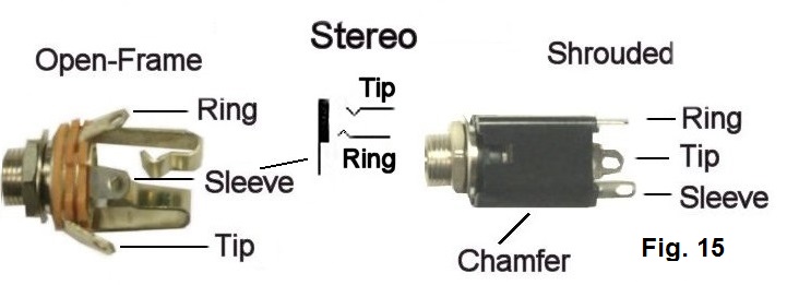
| The wiring is done, so let's connect input and output jacks. For testing purposes, we want to install input and output jacks as shown in Figure 13. The schematic shows mono jacks. This type has two contacts: tip and sleeve. Figure 14 shows the relationship between the schematic symbol and the physical item for two styles that you may encounter.. Figure 15 does the same thing for a stereo jack, which has three contacts: tip, ring and sleeve. The stereo jack shown is a Switchcraft #12B; note that the arrangement of the contacts may be different on other makes. | |||||||||||||||||||||||||||||||||||||||||||||||||||||||||||||||||||||||||||||||||||||||||||||||||||||||||||||
|
|
|||||||||||||||||||||||||||||||||||||||||||||||||||||||||||||||||||||||||||||||||||||||||||||||||||||||||||||
  |
|||||||||||||||||||||||||||||||||||||||||||||||||||||||||||||||||||||||||||||||||||||||||||||||||||||||||||||
| Solder short lengths of hookup wire to tip and ring of the jacks. If you add stiff ends and cover with heat shrink as with the battery connector that you made in the introductory article, you have convenient connectors that can be re-used for future jobs. Tip contact goes to the input capacitor and sleeve goes to ground. Figure 16 shows the setup for the NPN negative-ground build. Remember that the positive rail is ground if you are building PNP. Connect the battery and your gear. | |||||||||||||||||||||||||||||||||||||||||||||||||||||||||||||||||||||||||||||||||||||||||||||||||||||||||||||
|
|
|||||||||||||||||||||||||||||||||||||||||||||||||||||||||||||||||||||||||||||||||||||||||||||||||||||||||||||
| The "bite" of the Rangemaster is unmistakable. Make sure that the level
control works. If you don't hear the effect, go back over the layout and
look for something that's not connected correctly.
Also be sure that:
|
|||||||||||||||||||||||||||||||||||||||||||||||||||||||||||||||||||||||||||||||||||||||||||||||||||||||||||||
| |
|||||||||||||||||||||||||||||||||||||||||||||||||||||||||||||||||||||||||||||||||||||||||||||||||||||||||||||
| Tweaking Performance and Compensating For Transistor Gain | |||||||||||||||||||||||||||||||||||||||||||||||||||||||||||||||||||||||||||||||||||||||||||||||||||||||||||||
| |
|||||||||||||||||||||||||||||||||||||||||||||||||||||||||||||||||||||||||||||||||||||||||||||||||||||||||||||
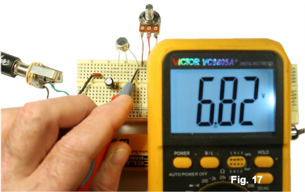
| If you bought my breadboarding kit for the RM, the transistor supplied with it is guaranteed to bias such that the voltage at the Collector falls between 6.6 and 7.2 volts--what I call the GEOFEX specification. This is shown in Figure 17. | |||||||||||||||||||||||||||||||||||||||||||||||||||||||||||||||||||||||||||||||||||||||||||||||||||||||||||||
|
|
|||||||||||||||||||||||||||||||||||||||||||||||||||||||||||||||||||||||||||||||||||||||||||||||||||||||||||||
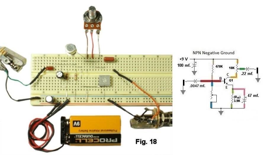
| If you are "rolling your own" and using a relatively low-gain transistor, you might have to adjust the value of Rb and/or Re to set the bias within spec. The procedure for doing this is described here at GEOFX.com. While trimming is not required for the transistor included with my kit, the kit includes suitable trimpots should you want to experiment with this adjustment. Figure 18 shows shows the NPN negative-ground layout with a trimpot substituted for Rb. | |||||||||||||||||||||||||||||||||||||||||||||||||||||||||||||||||||||||||||||||||||||||||||||||||||||||||||||
|
|
|||||||||||||||||||||||||||||||||||||||||||||||||||||||||||||||||||||||||||||||||||||||||||||||||||||||||||||
| Adding A Tone Stack | |||||||||||||||||||||||||||||||||||||||||||||||||||||||||||||||||||||||||||||||||||||||||||||||||||||||||||||
| This is a feature that the original RM didn't have. It has come to be
expected in boutique RM clones, with good reason, IMO: It makes the effect
way more flexible and is not hard to add. The added capacitance
in parallel with the input capacitor allows more or less low-end through to
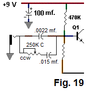
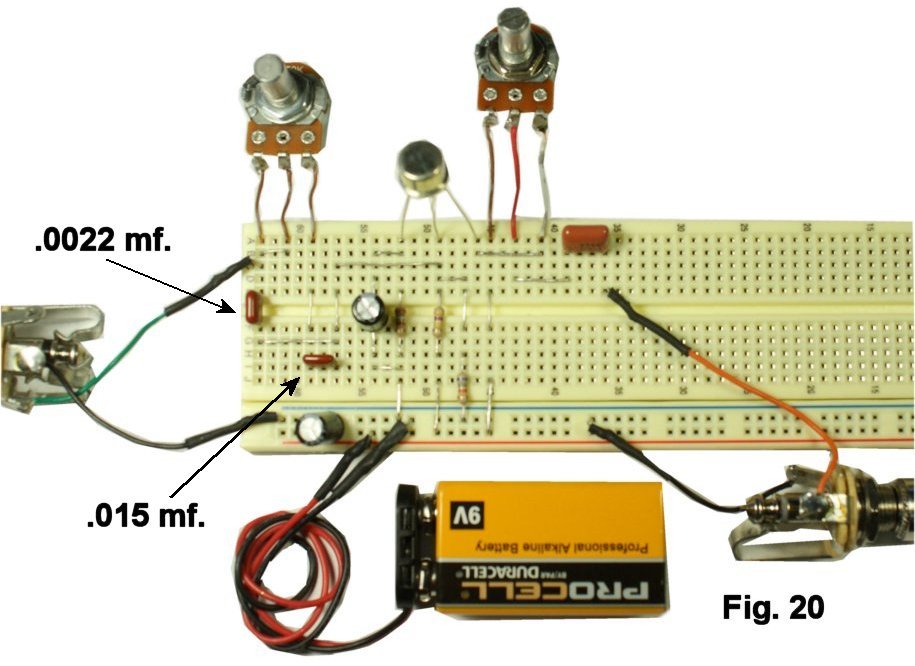
the Base, depending on the setting of the tone pot (Fig. 19 and Fig. 20).
To make it work as I wanted, I changed the input capacitor to .0022 mf. (marked 222). The added .015 mf. capacitor will usually be marked 153. Any 250K pot will work. However, I found that a reverse audio taper pot gave best "sweep" to my ears. "CCW" in Figure 19 means the "counter-clockwise" side of the pot. Follow the layout carefully or you will wonder why the sweep does not sound right. |
|||||||||||||||||||||||||||||||||||||||||||||||||||||||||||||||||||||||||||||||||||||||||||||||||||||||||||||
|
|
|||||||||||||||||||||||||||||||||||||||||||||||||||||||||||||||||||||||||||||||||||||||||||||||||||||||||||||
|
A Parts List This list shows everything that is included in my kit and is a reference for those who are rolling their own. It's everything needed to do what I have described to this point, including the LED demo in the intro article. |
|||||||||||||||||||||||||||||||||||||||||||||||||||||||||||||||||||||||||||||||||||||||||||||||||||||||||||||
|
|||||||||||||||||||||||||||||||||||||||||||||||||||||||||||||||||||||||||||||||||||||||||||||||||||||||||||||
| If you have the circuit working to this point, you have an idea of the relationship between a schematic and physical components on a breadboard. Congratulations! From here, you can either begin to commit to a soldered build or try some more experiments. | |||||||||||||||||||||||||||||||||||||||||||||||||||||||||||||||||||||||||||||||||||||||||||||||||||||||||||||
|
Darlington Pairs And The Oh My Darling(ton) Rangemaster |
|||||||||||||||||||||||||||||||||||||||||||||||||||||||||||||||||||||||||||||||||||||||||||||||||||||||||||||
| What Is A Darlington Pair? | |||||||||||||||||||||||||||||||||||||||||||||||||||||||||||||||||||||||||||||||||||||||||||||||||||||||||||||
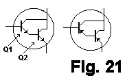
| It's two transistors, can be PNP or NPN, cascaded as in Figure 21.
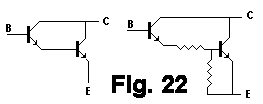
Transistor Q1 drives transistor Q2 directly, and the gains of the individual devices are multiplied; if Q1 has a gain of 30, for example, and Q2 a gain of 40, the gain for the pair would be 1200. The catch (there always is one, right?) is that both the leakage and the noise level of Q1 are also multiplied by the gain of Q2. So if Q1 leaks 30 microamps and Q2 has a gain of 40, the pair would leak over 1200. That would make proper biasing impossible, and operation would not be stable with temp, either. An arrangement that works for creating a usable device from such a pair uses two bias resistors to turn Q2 "off" just enough to bring the composite gain and leakage into workable ranges. The basic idea is shown in Figure 22. |
|||||||||||||||||||||||||||||||||||||||||||||||||||||||||||||||||||||||||||||||||||||||||||||||||||||||||||||
|
|
|||||||||||||||||||||||||||||||||||||||||||||||||||||||||||||||||||||||||||||||||||||||||||||||||||||||||||||
| Why Use A Darlington Pair? | |||||||||||||||||||||||||||||||||||||||||||||||||||||||||||||||||||||||||||||||||||||||||||||||||||||||||||||
| I started looking into Darlington pairs because decent germanium of suitable gain for the RM has continued to get scarcer and more expensive. While such parts remain available, I wanted a lower-cost alternative. In this case, both the present economics of the transistor market and Mother Nature cooperated. Low-gain germanium that was expensive back in the day is fairly cheap today, and low-gain parts are also often low in noise and leakage. If we take advantage and set up low-gain devices as Darlington pairs, it is perfectly possible to create "composite" devices that will function identically to more expensive individual parts. And the pairs can be NPN, making the resulting builds friendly to modern negative-ground power arrangements. Your "remainder" drawer may well be a source of suitable parts, as well as my Stock List. | |||||||||||||||||||||||||||||||||||||||||||||||||||||||||||||||||||||||||||||||||||||||||||||||||||||||||||||
|
|
|||||||||||||||||||||||||||||||||||||||||||||||||||||||||||||||||||||||||||||||||||||||||||||||||||||||||||||
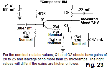
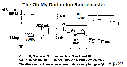
| The schem in figure 23 shows the biasing that I came up with by
experimenting. I refer to the resistors I added as Rc and Rd.
With trimming of the resistor values, the pair can easily be lined up to
bias at exactly 7.0 volts on the Collector of the composite device.
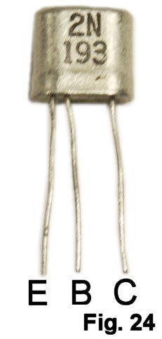
For the present, germanium transistors that will work well in this circuit remain readily available and cheap. However, this may only hold true until more people realize that you don't have to have particular type numbers of scarce parts to get a really good RM. Figure 24 shows one type that I have used successfully. I have noticed that some of these old Sylvania parts have the "2Nxxx" part number stamped such that the Emitter is on the left, while others are stamped on the opposite side. Follow the pinout and you won't go wrong. |
|||||||||||||||||||||||||||||||||||||||||||||||||||||||||||||||||||||||||||||||||||||||||||||||||||||||||||||
|
|
|||||||||||||||||||||||||||||||||||||||||||||||||||||||||||||||||||||||||||||||||||||||||||||||||||||||||||||
|
|
|
||||||||||||||||||||||||||||||||||||||||||||||||||||||||||||||||||||||||||||||||||||||||||||||||||||||||||||
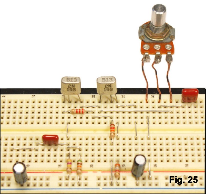
| Figure 25 shows what I actually laid out on the breadboard. I'm not walking through this one, so please refer to the intro article on breadboarding and the beginning of this article if you have questions about basic breadboarding technique. | |||||||||||||||||||||||||||||||||||||||||||||||||||||||||||||||||||||||||||||||||||||||||||||||||||||||||||||
|
|
|||||||||||||||||||||||||||||||||||||||||||||||||||||||||||||||||||||||||||||||||||||||||||||||||||||||||||||
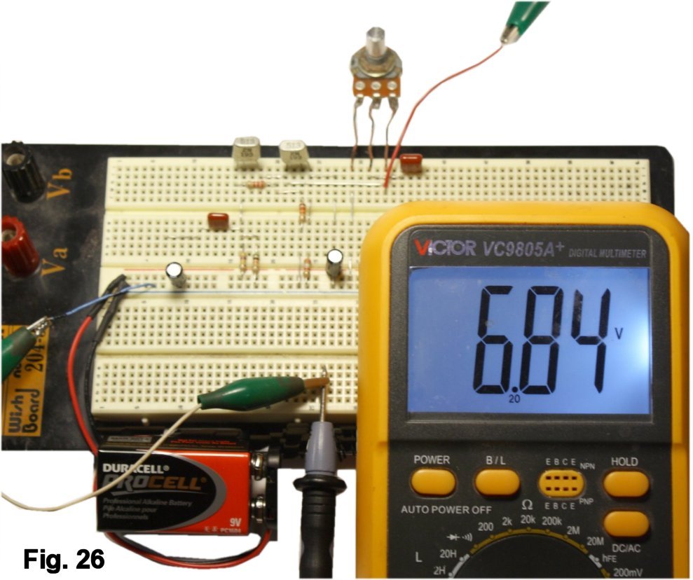
| I had adjusted the resistor values for the devices I was using, and the bias is pretty close to ideal (Fig. 26). Figure 27 shows what I actually built with the tone stack, anti-pop resistors and power protection diode. | |||||||||||||||||||||||||||||||||||||||||||||||||||||||||||||||||||||||||||||||||||||||||||||||||||||||||||||
|
|
|||||||||||||||||||||||||||||||||||||||||||||||||||||||||||||||||||||||||||||||||||||||||||||||||||||||||||||
|
If you are rolling your own or hunting through your remainder drawer, here are my suggestions for tweaking the bias and selecting transistors.
If you want to try these designs but need raw parts, please check my Stock List. I have lots of low-gain NPN and PNP germanium that remain from our sorting, and they are very reasonably priced. You may also be able to find suitable parts at auction or from the DIY Forums. |
|||||||||||||||||||||||||||||||||||||||||||||||||||||||||||||||||||||||||||||||||||||||||||||||||||||||||||||
| |
|
||||||||||||||||||||||||||||||||||||||||||||||||||||||||||||||||||||||||||||||||||||||||||||||||||||||||||||
| |
|
||||||||||||||||||||||||||||||||||||||||||||||||||||||||||||||||||||||||||||||||||||||||||||||||||||||||||||
| |
|
||||||||||||||||||||||||||||||||||||||||||||||||||||||||||||||||||||||||||||||||||||||||||||||||||||||||||||
|
|
|
||||||||||||||||||||||||||||||||||||||||||||||||||||||||||||||||||||||||||||||||||||||||||||||||||||||||||||
| |
|
||||||||||||||||||||||||||||||||||||||||||||||||||||||||||||||||||||||||||||||||||||||||||||||||||||||||||||
| |
|
||||||||||||||||||||||||||||||||||||||||||||||||||||||||||||||||||||||||||||||||||||||||||||||||||||||||||||
| |
|||||||||||||||||||||||||||||||||||||||||||||||||||||||||||||||||||||||||||||||||||||||||||||||||||||||||||||
| |
|||||||||||||||||||||||||||||||||||||||||||||||||||||||||||||||||||||||||||||||||||||||||||||||||||||||||||||
| |
|||||||||||||||||||||||||||||||||||||||||||||||||||||||||||||||||||||||||||||||||||||||||||||||||||||||||||||
| What's A Sziklai Pair? | |||||||||||||||||||||||||||||||||||||||||||||||||||||||||||||||||||||||||||||||||||||||||||||||||||||||||||||
| |
|||||||||||||||||||||||||||||||||||||||||||||||||||||||||||||||||||||||||||||||||||||||||||||||||||||||||||||
| |
|||||||||||||||||||||||||||||||||||||||||||||||||||||||||||||||||||||||||||||||||||||||||||||||||||||||||||||
| |
|||||||||||||||||||||||||||||||||||||||||||||||||||||||||||||||||||||||||||||||||||||||||||||||||||||||||||||
| |
|||||||||||||||||||||||||||||||||||||||||||||||||||||||||||||||||||||||||||||||||||||||||||||||||||||||||||||
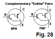
| This configuration was named for its
Hungarian originator. It's similar in concept to a Darlington, but it consists of a PNP and an NPN
transistor (Fig. 28). The devices inside the circle can be any of the ones we have discussed,
silicon or germanium. The designations outside the circle indicate how the
composite device will behave, and, by extension, how it should be powered and
biased.
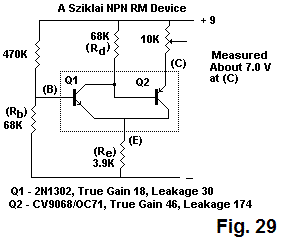
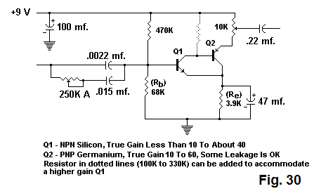
The NPN Sziklai pair is especially interesting, because it turns devices that you might normally not consider using into valuable parts. Q1 can be either germanium or silicon. Figure 29 shows an NPN germanium for Q1 and PNP germanium for Q2. I have successfully used a low-gain silicon "dot" for Q1 (Fig. 30), and you can find other possibilities on my Stock List, like the 2N2369A or 2N3440.
|
|||||||||||||||||||||||||||||||||||||||||||||||||||||||||||||||||||||||||||||||||||||||||||||||||||||||||||||
| |
|
||||||||||||||||||||||||||||||||||||||||||||||||||||||||||||||||||||||||||||||||||||||||||||||||||||||||||||
|
This setup used NPN germanium for Q1 and PNP germanium for Q2. |
|||||||||||||||||||||||||||||||||||||||||||||||||||||||||||||||||||||||||||||||||||||||||||||||||||||||||||||
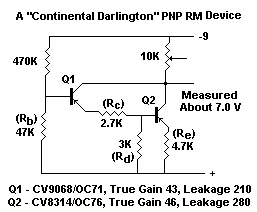
| PNP devices will work fine also; just remember to reverse all polarities. Gains of these usually run a little higher, so there will be some more tweaks to the bias. Here is a typical setup that I did with a couple of European OC7x types (Fig. 32). | |||||||||||||||||||||||||||||||||||||||||||||||||||||||||||||||||||||||||||||||||||||||||||||||||||||||||||||
|
|
|||||||||||||||||||||||||||||||||||||||||||||||||||||||||||||||||||||||||||||||||||||||||||||||||||||||||||||
|
Where To Go From Here Now that you have a circuit working, check out the article in Projects. You already have usable transistors, and you can buy a full kit, or pieces, or just a PC board depending on how you want to build. Thanks to R. G. Keen for his helpful suggestions and consulting! Questions and comments are welcome at smallbearelec@ix.netcom.com. |
|||||||||||||||||||||||||||||||||||||||||||||||||||||||||||||||||||||||||||||||||||||||||||||||||||||||||||||