Breadboard A Vintage IC Distortion
© 2020 By Small Bear Electronics LLC
Some years ago, I worked up this breadboarding tutorial for an IC-based distortion similar to an MXR Distortion + or a BOSS DS-1. I know from customer feedback that it was helpful to many beginners. However, one of the ICs that I recommended at the time has gone extinct. The design also needs a JFET, and some types that were long common are now only available in surface-mount packaging. This revision uses through-hole parts that I have in good stock and includes suggestions for using types that you may find locally.
If you have never used a solderless breadboard, please refer to the intro article before you continue on here. That How-To covers a lot of basic information and techniques; I presume that you have been through it, have done the demos, understand how the tool works and have started learning to use your multimeter. If you are already familiar with breadboarding, note that the level of detail in this article is meant to guide complete beginners, so please be a little patient.
For a demo at this level, I think the MXR Distortion + a little too easy. But the BOSS DS-1, even with all its switching circuitry stripped out, contains more components than I think a beginner would be comfortable with setting up. So this variant uses an FET (Field Effect Transistor) input stage to reduce the complexity. I'm sure you will like the result, and you will learn enough in setting it up to breadboard lots of other distortions and try out mods.
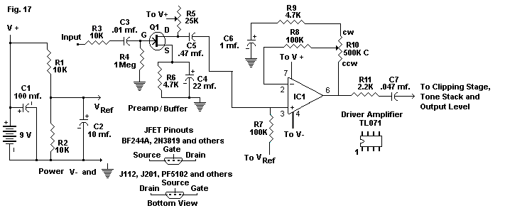
Here's the basic circuit that we will set up:
I have purposely not included jacks, stomp switch or power switching in order to keep it simple; we'll add those later. This schem is a lot more complex than the LED demo, but don't let it scare you; it breaks down easily to separate functional blocks, and I'll walk you through it slowly. We'll stop at key points and do some tests and demos to make sure things are working and learn what the various sections do.
Here are few rules that will help with interpreting the schem:
Where wires cross in a schematic but Don't connect, you'll see
this: ![]()
Where wires cross or join in a schematic and Do connect,
you'll see this:
![]()
The Ground symbol
![]() is not a
connection to the Earth; it's a reference point from which voltages in
the circuit are measured. All points in the circuit that have or share the
Ground symbol are connected. If this is not clear yet, you'll get the idea as
I walk you through the build.
is not a
connection to the Earth; it's a reference point from which voltages in
the circuit are measured. All points in the circuit that have or share the
Ground symbol are connected. If this is not clear yet, you'll get the idea as
I walk you through the build.
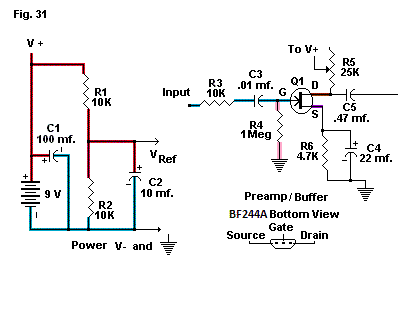
Let's set up the reference voltage (V ref) section at the lower left, and then we'll give beginners a look at what it does and why it is needed.
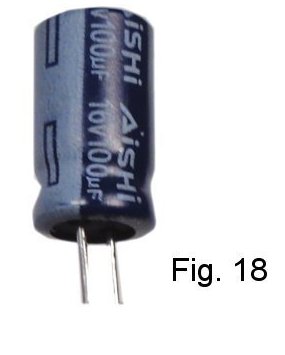
Trim the leads of a 100 mf. electrolytic capacitor, following the convention of leaving 1/4" to 5/16" of lead length for insertion in the board. Electrolytic caps are most often polarized; on radial-case types like this one, a black band marks the negative side (Fig. 18.)
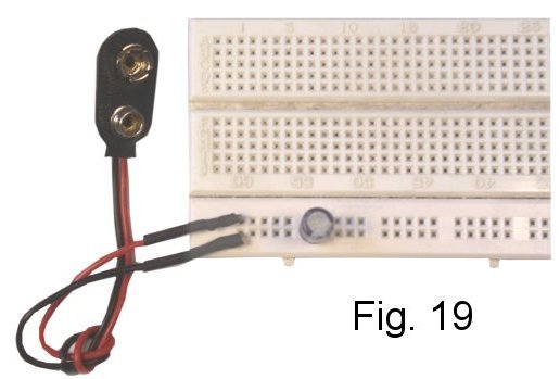
You may want to follow my directions and layout this time around; once you have the idea, you're free to do whatever works. Similarly, I am working from left to right on the board, but that's not engraved in stone, either. Plug in the cap with the negative side to the negative power bus (Fig. 19.) You don't have to use exactly the same locations I do. However, if following my footsteps (bear tracks?) helps to build your confidence and avoid mistakes, go for it. Fig. 20 shows the connections you have made.
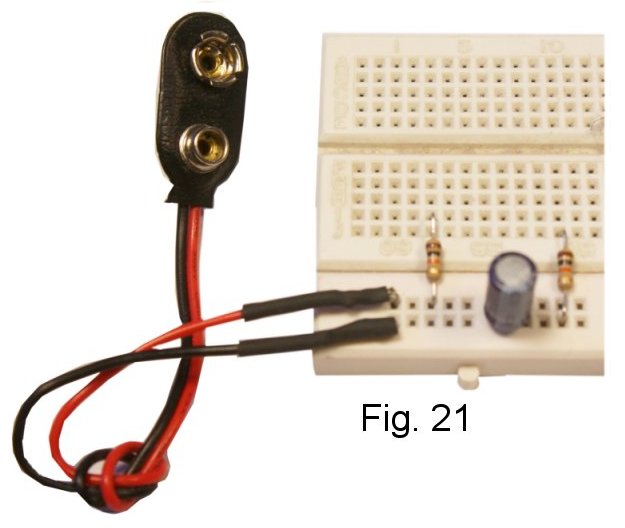
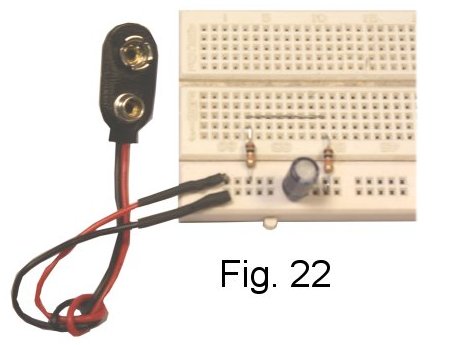
Now set up the voltage divider R1, R2. Both resistors are 10K, color code Brown, Black, Orange, Gold. Start with R1; clip its leads and form them to span the distance from the positive power supply bus to the second hole in the fifth column. On this breadboard, that is index I58. Follow with R2 from the negative supply bus to the first hole in column 51 (Fig. 21). Add a bare wire jumper to connect R1 and R2 (Fig. 22), and Fig. 23 shows where we are at. Got the idea?
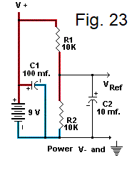
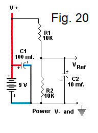
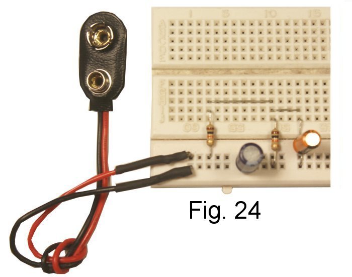
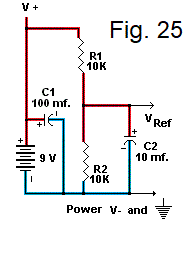
Finish this section by adding C2, a 10 mf. radial electrolytic. This goes from the junction of R1 and R2 to the negative supply bus, so create a bare wire jumper spanning four holes and form the leads of the capacitor to span the distance to the bus (Fig. 24.) Observe polarity when inserting the capacitor! The junction we have just created is Vref in the schematic (Fig. 25.).
Just a note: Because this is a first project for many people, I have been very prescriptive about exactly how to locate components and jumpers. Also for the sake of clarity, the physical layout is very precise and all wiring is squared off. As you do your own experimenting, this need not be the case if it isn't convenient or you need to get something done quickly. Breadboarding as I show it here makes documenting your work much easier and mistakes more clearly evident, so it's worth learning this way from the start.
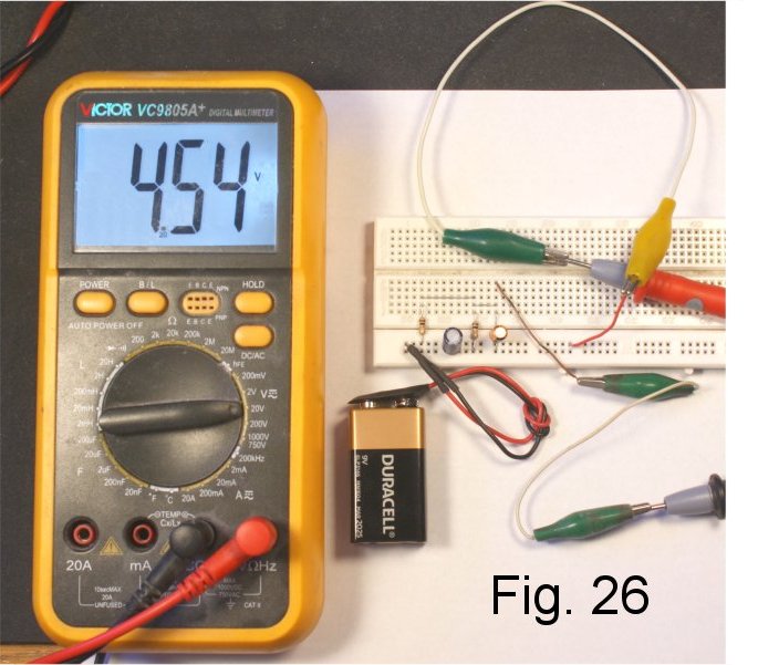
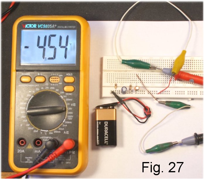
The power distribution section is done. For a look at what it does, fire up your multimeter and connect the battery. Set the meter to measure DC volts in a low range, and connect the negative meter lead to the Vref point. Use a short length of wire to help with making the connection. Now measure the voltage at the positive supply bus (Fig 26.) We are seeing about half of the battery voltage, and a look at the schematic tells us why. Resistors R1 and R2 are both 10K. In the way Ohm's Law works, the battery "drops" a proportionate 50% of its voltage across each of two equal value resistances. If you now shift the positive meter lead to the negative power supply bus, you will see exactly the same voltage, but the meter will read it as Negative 4.xx volts (Fig. 27.)
Why do we need to do this? Again, look at the full schematic. Like most op-amp chips, the one we use wants to see two supply voltages--one positive and one negative--with respect to a reference point. We actually could provide V+ and V- by using two batteries, but that gets awkward for a pedal. So this circuit dodge (which you will see in thousands of pedal schematics) is used to, essentially, fool the chip into seeing what it must in order to work.
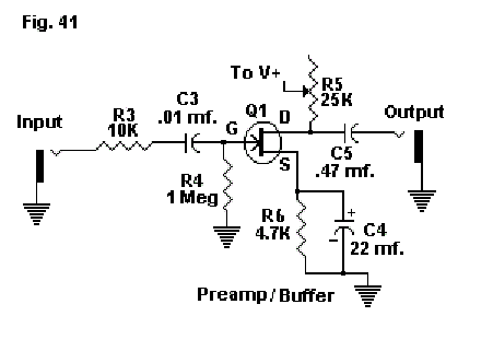
Now let's talk about the Junction Field-Effect Transistor (JFET) stage, which comprises Q1 and its associated parts.
As I mentioned earlier, this input stage differs from most BOSS designs. Most BOSS pedals, including the DS-1, use two NPN bipolar transistors at the input. The first is connected as an emitter follower, and the second as a common-emitter amplifier. The emitter follower presents a high input resistance for a guitar, and the second stage boosts the signal enough to drive whatever follows. While Roland has good technical reasons for doing things this way, my priority was getting a similar result with fewer components. The JFET stage (which I actually lifted from the BOSS FA-1) does a nice job of this.
The OEM part in the FA-1 was a 2SK246-GR. It's long obsolete and has become hard-to-find, because the stock on the surplus market was bought by people who clone the FA-1. Fortunately, there is nothing exotic about it. I have suggested as subs a few types that I have tested in the circuit, can supply and know to be commonly available elsewhere, at least at this writing.. The only thing you must be aware of is that not all devices have the same pinout. I show in the schematic the pinouts for the devices I used; if you are using something else, check an on-line reference for the pinout and change the breadboard connections accordingly if necessary. I will continue with setup directions using the BF244A and then include a photo that shows the layout using the J201 and similar devices.
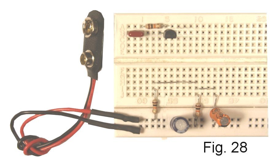
Install the transistor with its Gate (middle lead) in the seventh column, second row. On my breadboard, this happened to be index B5. The flat side faces the power supply bus. Then add input capacitor C3 (.01 mf., marked "103") and input resistor R3, 10K, color code Brown, Black, Orange, Gold. If you happen to be using a physically larger capacitor than the one I show for C3, there is ample room for it. Fig. 28 shows the layout, and Fig. 29 shows the connections you have made.
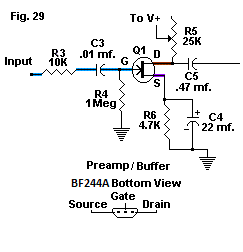
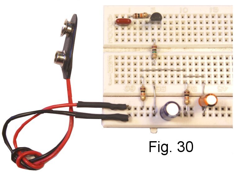
Now add resistor R4, 1 Meg, color code Brown, Black, Green, Gold, and a jumper to connect it to the negative supply bus. See Fig. 30 and Fig. 31.
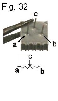
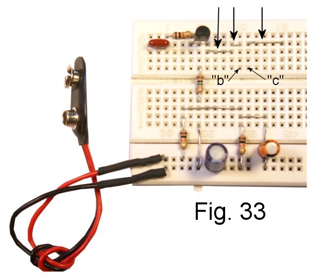
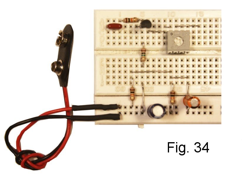
A trimpot is a potentiometer that is specifically made to be mounted on a board and adjusted with a screwdriver when the exact resistor value needed is not certain. R5, a 25K cermet (metal film) type, is used to adjust the Drain current through the JFET. It has three terminals like any regular pot, but we only need to connect to one of the end terminals (a or b in Fig. 32) and the wiper (c). Before you plug in the trimpot, install three short jumpers as shown in Fig. 33. Plug in the trimpot, making sure that terminal "b" and terminal "c" go in at the points shown. The layout now looks like Fig 34.
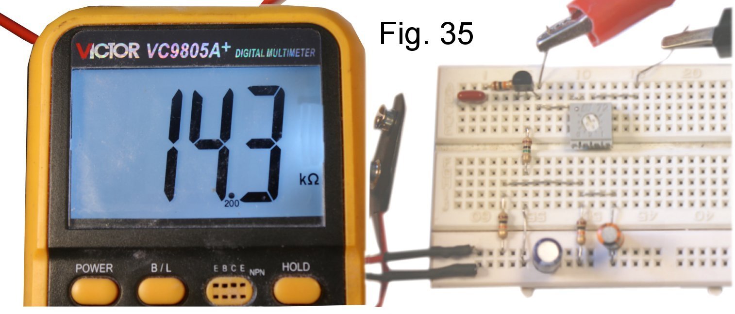
To make sure that the trimpot is plugged in correctly, a insert short leads as shown in Fig. 35. Set your meter to resistance, and watch the resistance change when you take a screwdriver to the trimpot. If nothing happens, check out how you have plugged in and connected the trimpot.
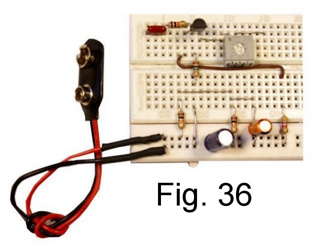
To make the source pin of the transistor available on the right side, thread a short piece of insulated wire in the channel of the board and terminate as shown. Add resistor R6, 4.7K, color code Yellow, Violet, Red, Gold. The layout is shown in Fig. 36.
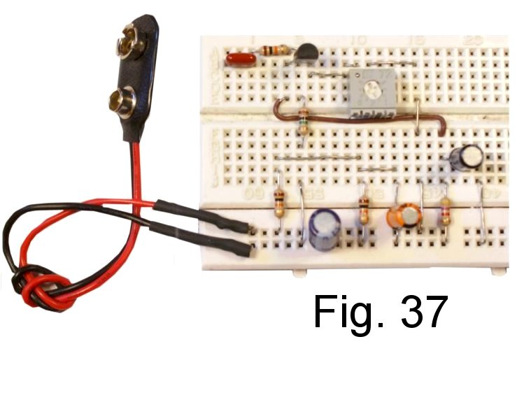
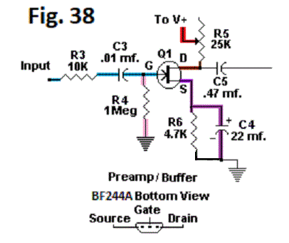
Add the two jumpers that connect one side of the trimpot to V+, then add the 22 mf. electrolytic capacitor C4 and its jumper to ground (Observe polarity!). See Fig. 37 for the layout and Fig. 38 for what has been connected in the schematic.
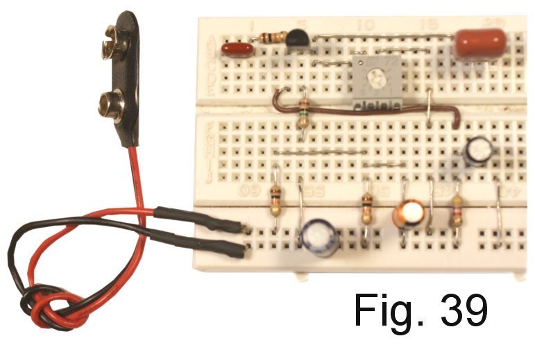
Capacitor C5, .47 mf., will usually be marked 474K. Add a jumper to connect to the Drain of the transistor, and then plug in C5. See Figure 39.
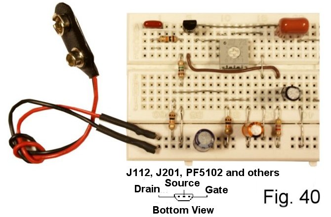
For those using a J201 or other device with a G S D pinout, Fig. 40 shows the completed layout. The circuit does not change at all--only the layout does to accommodate the different pin arrangement. To get oriented, start by placing the transistor with its middle (Source) lead in the seventh hole, second row. The flat side of the device faces away from the power busses.
The preamp/buffer is finished, and we can run an initial test before adding the driver amplifier. The pics that follow show the preamp using the BF244A, but the J201 version will work equally well.
For testing purposes, we want to install input and output jacks.
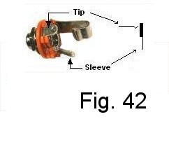
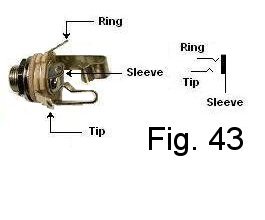
The schematic Fig. 41 shows mono jacks. This type has two contacts, tip and sleeve. Figure 42 shows the relationship between the schematic symbol and the physical item. Figure 43 does the same thing for a stereo jack, which has three contacts: tip, ring and sleeve. The stereo jack shown is a Switchcraft #12B; note that the arrangement of the contacts may be different on other makes.
In a typical pedal build, we would use a stereo jack for the input and connect the ring contact to switch battery power. To keep things simple here, we use only the tip and sleeve. Connect a short length of shielded cable to each jack, making sure that the shield is soldered to the sleeve. (Ordinary insulated wire will work, but shielded cable reduces some of the noise inherent in an open layout like this.) Add bare wire terminations to the ends that go to the breadboard just as you did for the battery snap.
The shields are plugged to the ground bus. Input tip goes to the 10K resistor R3, output tip to capacitor C5.
Are you ready? Connect up your guitar and an amplifier. Connect your multimeter set to measure DC voltage, negative side to the ground bus and positive side to the Drain of the JFET. Set the trimpot to about the middle of its range, and and connect a 9-volt battery or filtered power supply. Figure 44 shows the setup, and what I saw.
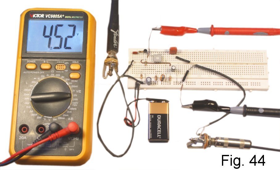
If the trimpot is set anywhere near its midpoint, you should hear the guitar clearly, and the voltage should be somewhere between 3.5 and 5.5 volts. If you can't get the voltage down into this range, try lowering the source resistor, R6, to 2.2K. Now adjust the trimpot so that the Drain voltage is around 4.5 volts. You should be getting a clean volume boost. Want to prove it? Move the lead from the output jack tip off its connection to C5 and to a hole in an unused column. Then connect a short lead from that column back to the tip of the input jack. Play, and briefly switch the amplifier connection between the unboosted guitar and the output from C5. (The input resistance is so high that this preamp doesn't suck tone, so don't be concerned that the circuit is not fully bypassed.) Hear the boost?
If you don't hear the boost or you can't properly set the voltage, Check Your Wiring. I have proceeded exactly as shown here, so you should be duplicating my results when everything is correct.
If you are with me so far, let's set up the driver stage.
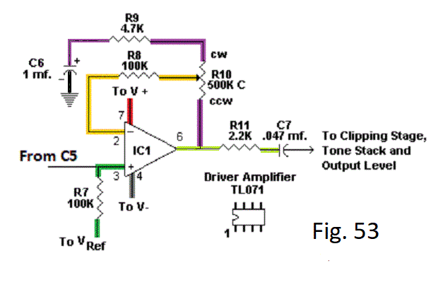
The TA7136P that was OEM in the DS-1 became scarce long ago. This build uses a TL071, which is readily available and inexpensive and works well. Start the layout by finding a convenient place to plug in the chip.
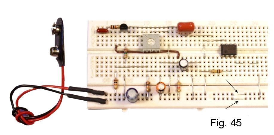
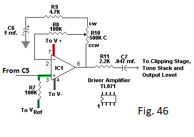
Make the connections to V+ and V-, add the 100K resistor on the input pin 3 and jumper the other side of the resistor to Vref (Fig. 45, Fig. 46). Note the two jumpers on the power bus; many breadboards split the power bus, and so jumpers are needed to connect the halves. A quick continuity test with your multimeter will tell you whether you need to make this connection..
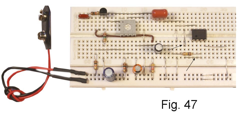
Make the connection from C5 to pin 3 of the IC (Fig. 47).
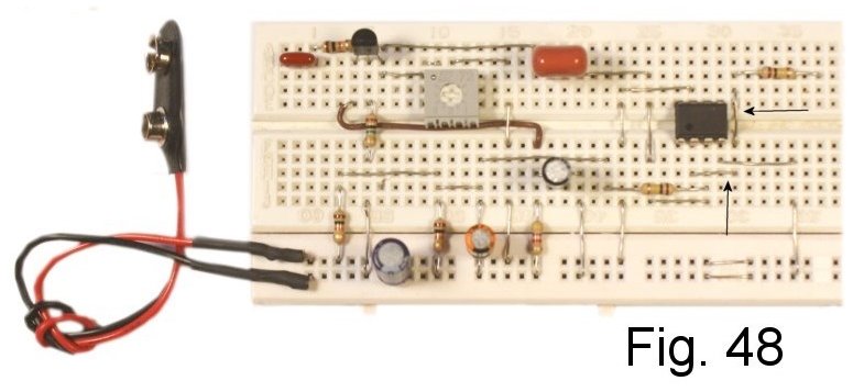
Add a 100K resistor spanning seven holes, and jumpers to connect one side to pin 2 (Fig. 48, Fig. 49)
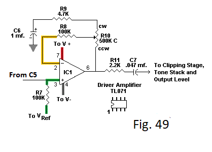
Potentiometer R10 (500K reverse audio taper, which is what the "C" indicates) together with Resistors R8 and R9, set the gain of this stage. Prepare the potentiometer for connecting to the breadboard by soldering leads to it. A few inches of insulated breadboarding wire to each terminal is fine. By convention, we refer to the terminals of the pot as CCW (counter-clockwise), W (wiper, for the moving contact) and CW (clockwise). Plug in the potentiometer and add resistor R9, 4.7K, color code Yellow, Violet, Red, Gold. The connections to the potentiometer are:
CCW to pin 6 of the chip, jumper needed
Wiper to one side of R8
CW to resistor R9
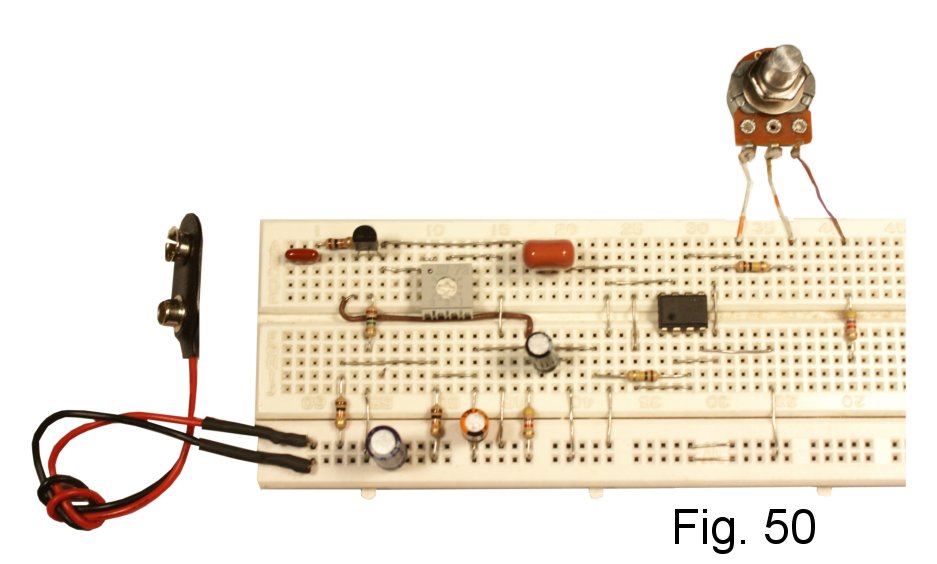
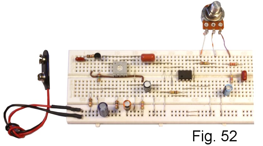
See Fig. 50 and 51.
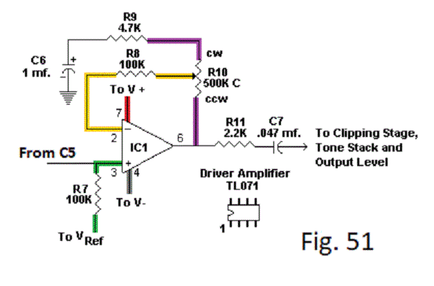
Add resistor R11, 2.2K, color code Red, Red, Red, Gold. That needs a jumper to the CCW side of the pot. Add electrolytic capacitor C6, observing polarity--negative side to V-. Finish up with output capacitor C7, .047 mf., usually marked 473K. See Fig. 52 and 53.
Testing The Driver Stage
Once again, connect your guitar and amplifier. The output tip connects to C7. Set the amplifier volume very low and start with potentiometer R10 fully counterclockwise. Connect the battery.
Notice how loud the guitar is even with R10 fully counterclockwise and the amplifier low? Turn R10 a little bit clockwise and the circuit will break into feedback. If you are with me to this point, we are ready to add some distortion. If you don't hear LOUD guitar, check your wiring.
Distortion - Adding a Diode Clipping Stage
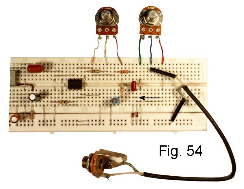
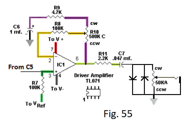
If the circuit is working to this point, disconnect the battery and the output jack temporarily. Insert two 1N914 diodes connected back-to-back (the bar side on the case is the bar side in the schematic) and a 50K audio potentiometer to control the output level. (Don't miss the short jumper that joins the diodes). Return the diodes and the CCW side of the potentiometer to ground. Fig. 54 and Fig. 55 show what this looks like.
With both controls fully counterclockwise, re-connect the battery and the output jack.
With your amplifier at a moderate playing level, rotate the level pot till you hear fairly loud guitar. Now bring up R10. Got distortion?
CONGRATULATIONS!
I don't discuss much theory in these tutorials, because the "Why" is covered extensively in references done by people who know far more than I do. But I'll make an exception for the question that I know just occurred to you: How come it takes so many components to get to this point, and only two diodes to create the distortion?
The answer is that the stages prior to the diodes are needed to boost the signal from the guitar pickup (10-20 millivolts) to a level sufficient to make a diode conduct. A diode conducts in one direction only, and it won't even do that unless the voltage across it exceeds its "forward conduction voltage." This is about 200 mV for germanium diodes and about 600 mV for most silicon diodes. Notice from the schematic that the diodes are connected directly across the signal output. So when one half-cycle of the guitar signal exceeds the forward conduction voltage, the diode conducts any part of the signal greater than that voltage directly to ground. The same thing happens with the opposite half cycle. Your ear perceives as distorted the "clipped-off" signal that results. Advancing R10 raises the signal level into the diodes, which increases the amount of signal that is clipped and so the distortion.
What To Try Next
If you just do a Google search on "DS-1 Mods," you will get numerous links that describe subs for the IC, coupling capacitors, the clipping diodes and the tone stack of that pedal. Not everything will be applicable to this build, but much will. One very simple, but interesting, mod is to substitute a germanium diode for one of the 1N914s. Germanium clips at a much lower voltage than silicon, so using one of each results in an output that isn't symmetrical. Many people find that they like this timbre. While 1N34a is often specified, any type number will do, and some will sound slightly different from others because of differences in manufacture. Other silicon types like the 1N400x are candidates, as are various LEDs. The links will lead you to hundreds of ways to set up clipping diode stages, and the components needed are mostly easy-to-find and cheap.
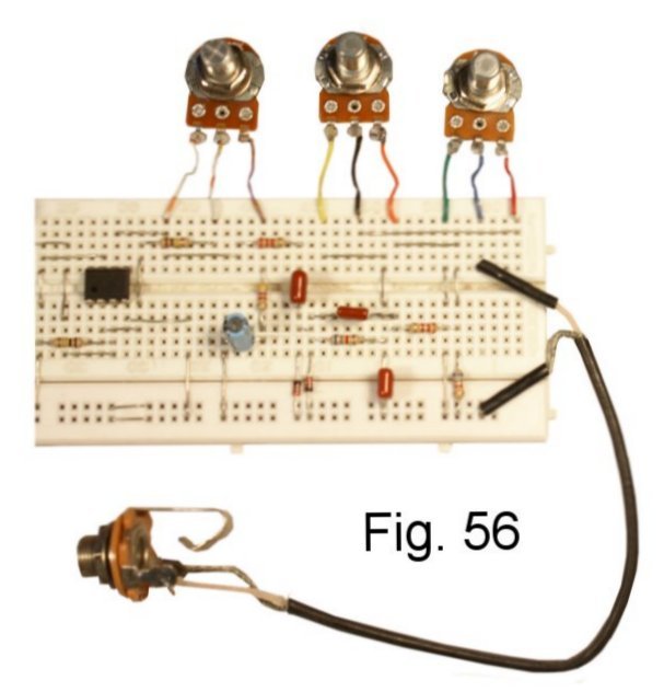
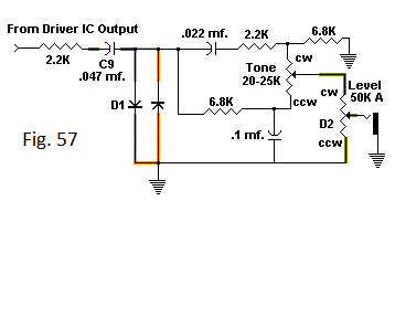
Oh yeah...the tone stack. Adding the ability to cut or boost treble widens the tone palette by light-years. I have used the DS-1 tone stack satisfactorily in other builds, and I suggest it here as well, with one Small Bearish spec: Many DIY builds list a 25K linear pot for the tone control, but that taper isn't ideal. The kit we offer includes a 20K pot with a "W" taper, which is the same taper Roland/BOSS uses. It gives much better control on the treble side. Start by removing the level pot and its three jumpers. Install the tone and level pots as shown in Fig. 56. Fig. 57 shows the schematic of the tone stack following the diodes and before the level control. If you have been with me so far, you should be able to add the tone stack components on your own. When done, plug in your gear again and try out the controls.
I hope you enjoy coming up with a version of this build that you want to commit to solder. I'll be doing that myself in a future article. Following is a list of parts needed to do everything shown above, including the LED demo in the intro article.
| Quantity | Description | SBE Stock List SKU |
| Resistors - All 1/4-watt 5% Carbon Film | ||
| 3 | 10K | 0900, 0901, etc. |
| 2 | 4.7K | |
| 2 | 100K | |
| 2 | 2.2K | |
| 2 | 6.8K | |
| 1 | 1 Meg | |
| Potentiometers and Trimmers | ||
| 1 | 500K Reverse Audio | 1007 |
| 1 | 50K Audio | 1005A |
| 1 | 20K W Taper | 1007 |
| 1 | 25K Cermet Trimmer | 1015 |
| Capacitors | ||
| 1 | .01 mf. 50 Volt Polyester Film | 1101B or 1150 |
| 1 | .47 mf. 50 Volt Polyester Film | 1105 |
| 1 | .047 mf. 50 Volt Polyester Film | 1101B or 1150 |
| 1 | .022 mf. 50 Volt Polyester Film | 1101B or 1150 |
| 1 | .1 mf. 50 Volt Polyester Film | 1101B or 1150 |
| 1 | 1 mf. 16 Volt Radial Electrolytic | 1400 |
| 1 | 10 mf. 16 Volt Radial Electrolytic | |
| 1 | 22 mf. 16 Volt Radial Electrolytic | |
| 1 | 100 mf. 16 Volt Radial Electrolytic | |
| ICs, Transistors and Diodes | ||
| 1 | BF244A, 2N3819 or similar | 2107 |
| 1 | TL071 | 1528 |
| 1 | LED 5mm High-Brightness Red | 2302 |
| 2 | 1N914 | 2208 |
| 1 | Germanium Diode 1N34a or similar | 2209 |
| Wire and Tubing | ||
| Bare Tinned Copper Wire, #22 or #24 | 0509 | |
| Insulated Tinned Copper Wire, #22 or #24 | 0508M | |
| Shielded Cable | 0510 | |
| 1/16" heat shrink | 0500 | |
| Jacks, Fittings | ||
| 1 | Mono Jack, Switchcraft #11 | 0600 |
| 1 | Stereo Jack, Switchcraft #12B | 0602 |
| 1 | 9-Volt Battery Snap | 0619 |
| Tools | ||
| 1 | Breadboard or Breadboard Strip | 2700, 2700A, 2700B |
| 1 | Multimeter | 2701, 2701A |