Biasing JFETS - Breadboard A Bare-Ass Boost
If you have never used a solderless breadboard, please refer to the intro article on breadboarding before you continue. That How-To covers a lot of basic information and techniques; I presume that you have been through it, have done the demos, understand how the tool works and have started learning to use your multimeter. If you are already familiar with breadboarding, note that the level of detail in this article is meant to guide complete beginners, so please be a little patient.
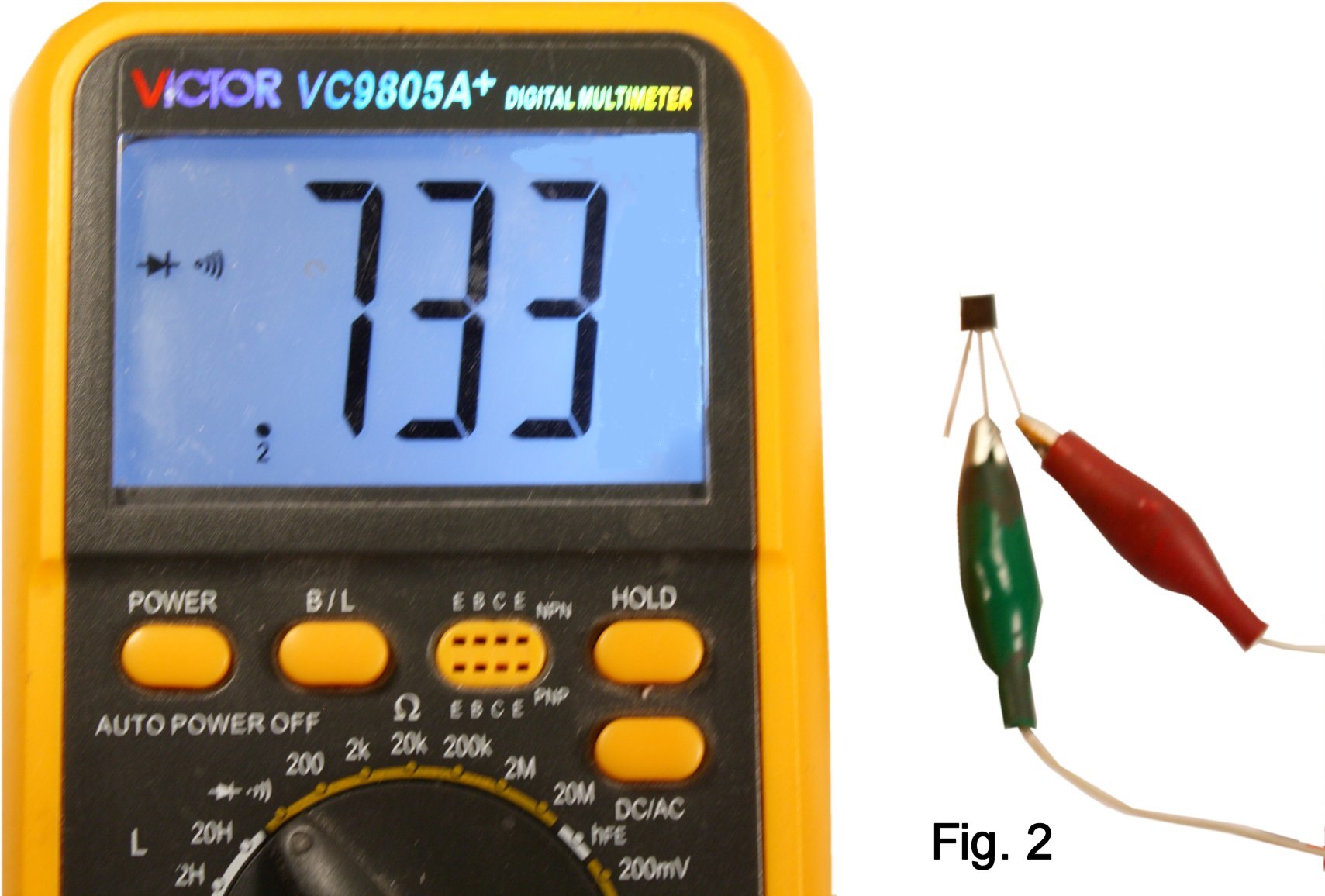
It occurred to me that since we have a p-n junction, the Gate-To-Drain and Gate-To-Source ought to behave as silicon diodes, and so they do (Fig. 2).
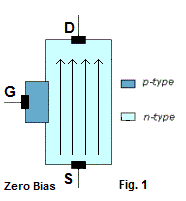
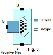
A "depletion region" (Fig.3) is created that progressively chokes off current flow through the channel. If the reverse bias is high enough, almost no current flows. A relatively small change in the bias voltage causes a relatively large change in the current through the channel, so the JFET can function as an amplifier or switch.
-
Where wires cross in a schematic but Don't connect, you'll see this:

-
Where wires cross or join in a schematic and Do connect, you'll see this:

-
The Ground symbol
 is
not a connection to the Earth; it's the reference point from which all
voltages in the circuit are measured. All points in the circuit that have or
share the Ground symbol are connected. If this is not clear yet, you'll get
the idea as we go further.
is
not a connection to the Earth; it's the reference point from which all
voltages in the circuit are measured. All points in the circuit that have or
share the Ground symbol are connected. If this is not clear yet, you'll get
the idea as we go further.
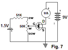
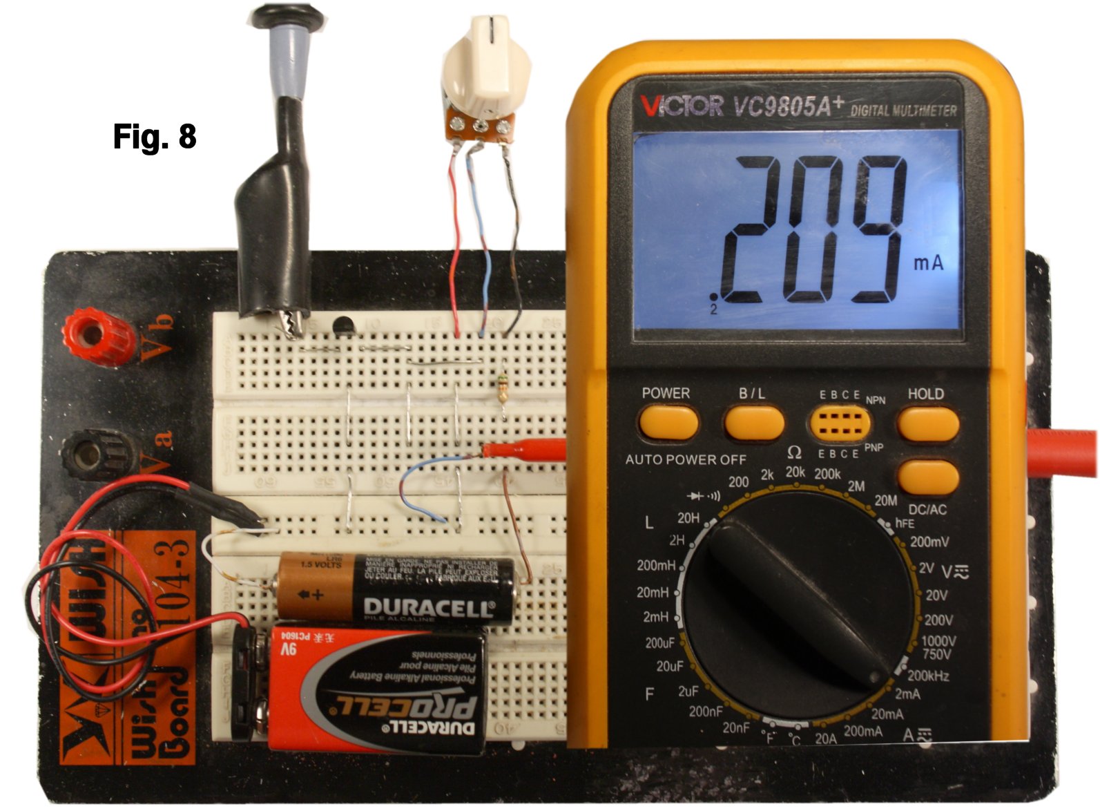
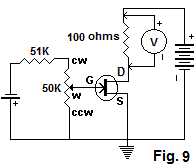
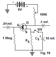
The 51K resistor and the 50K pot are connected as a voltage divider; since they are roughly equal in resistance, half the battery voltage is dropped across the resistor and half across the pot. The gate of the JFET is connected to the wiper so, as the wiper goes more clockwise (CW), it will see from zero to about .75 volts negative with respect to ground. Figure 8 shows the pot about half-way clockwise and the Drain current considerably lowered. The voltage at which the channel is closed and drain current is minimum is the pinchoff voltage, Vp .
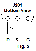
If you bought the breadboard kit, it includes two devices for which Vp has already been measured by the method shown here. The J201 in the kit will have a Vp of -1.0 V or smaller. If you are doing a similar demo using your own J201s, be aware that Vp for that part can be as high as -1.5 V. To test parts with a Vp between -.75 V and -1.5 V, leave out the 51K resistor. Other popular devices, like the 2N5457, for example, can have a Vp of -6 volts or greater. For those, use a 9 volt battery rather than the AA penlight.
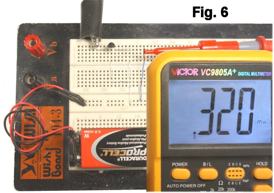
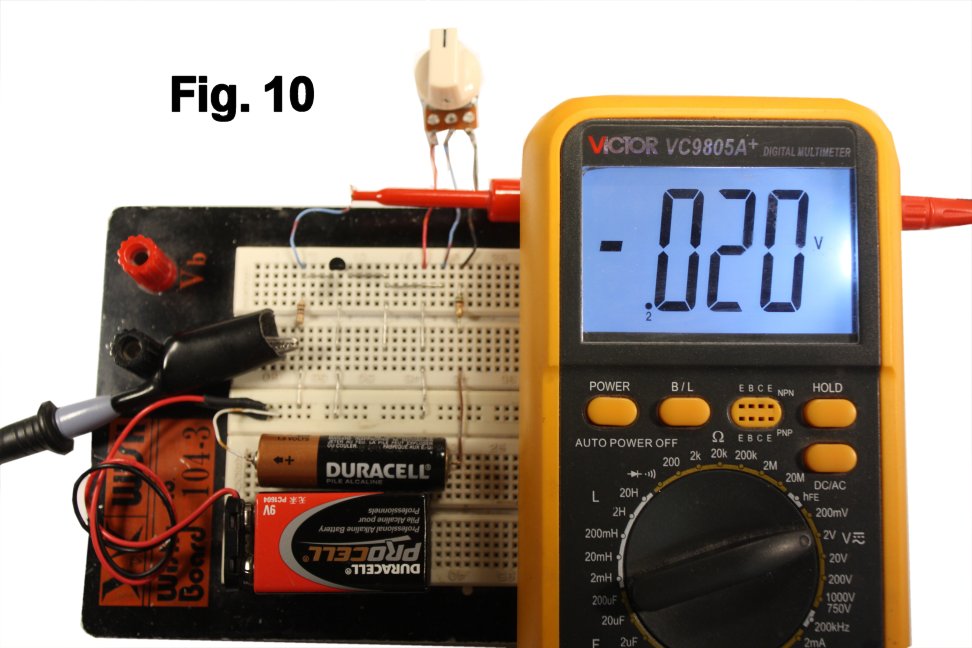
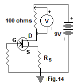
For example, say that .2 ma. (.0002 amp) or thereabouts is flowing in the drain circuit as shown above. By Ohm's law, the voltage drop across the 100 ohm resistor is I * R or .0002 * 100 = .02 volts. And that's what it is when I actually measure it (Fig. 10). Multiplying the voltage reading by 10 expresses the current in ma.
Call me obsessive...I actually graphed my data and got a slope like figure 12.
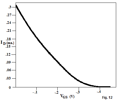
| Bias | ID |
| -0 V | .32 ma. |
| -.02 V | .29 ma. |
| -.04 V | .27 ma. |
| -.06 V | .25 ma. |
| -.08 V | .22 ma. |
| -.1 V | .2 ma. |
| -.12 V | .19 ma. |
| -.14 V | .17 ma. |
| -.16 V | .15 ma. |
| -.18 V | .14 ma. |
| -.2 V | .12 ma. |
| -.22 V | .11 ma. |
| -.24 V | .10 ma. |
| -.26 V | .09 ma |
| -.28 V | .07 ma. |
| -.3 V | .06 ma |
| -.32 V | .05 ma. |
| -.36 V | .03 ma. |
| -.38 V | .02 ma. |
| -.4 V | .01 ma. |
| -.43 V | 0 ma. |
.08 /.1 = .8 Millisiemens or .0008 Siemens
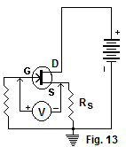
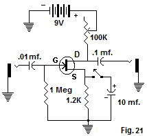
The resistor from the gate to ground will be a very high value--typically 1 Meg or more. It allows the gate to "see" ground, but no voltage is dropped across it because current doesn't flow into the gate. In the drain circuit, we know that current flows from drain to source. By putting a small resistor RS between the source and ground, the gate becomes effectively negative with respect to the source by the amount of the voltage drop (ID * RS) across the resistor.
Looking at the graph and the data in figure 11, I chose to set the bias at -.18 V, which puts ID at .14 ma. (.00014 amp). By Ohm's law, the required resistance is then: .18 / .00014 or 1285 Ohms.
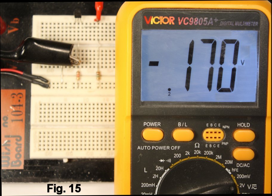
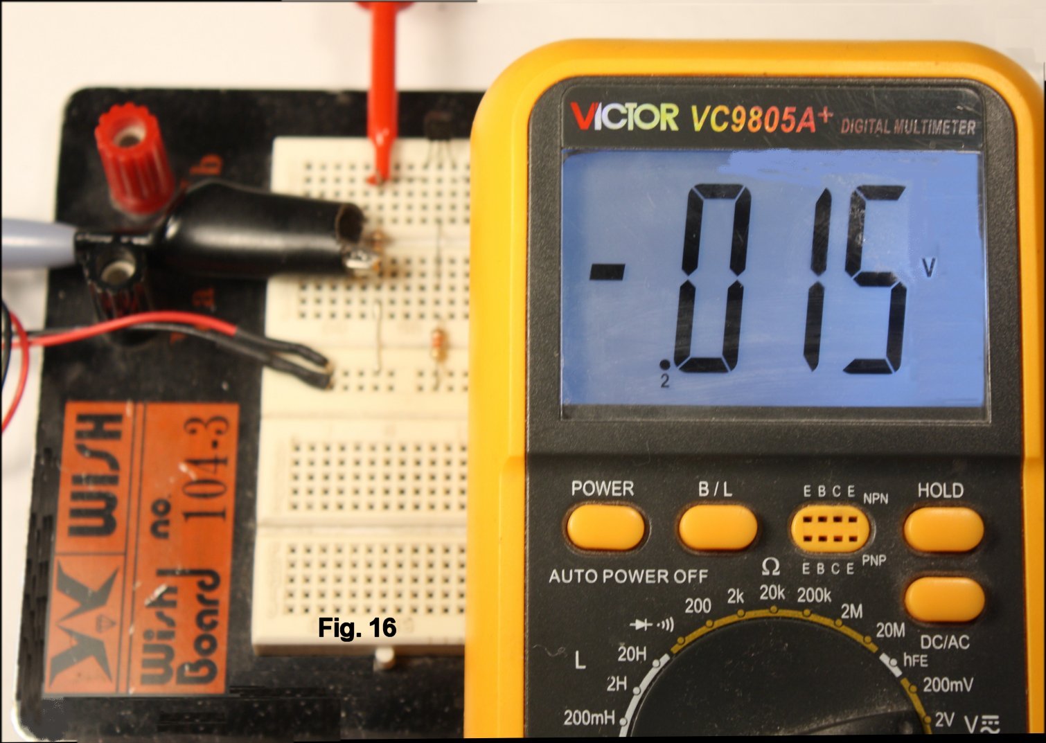
We could use a 1% resistor to get really close, but that is not necessary for most practical purposes. I set RS at 1.2K, the nearest standard value in 5% tolerance and added the 100 ohm resistor to be able to easily measure ID (Fig. 14). As you can see from the readings in Fig. 15 and Fig. 16, the bias is almost spot-on.
The breadboard kit includes a range of 5% carbon film resistors from which to select a value that sets ID close to half of IDSS.
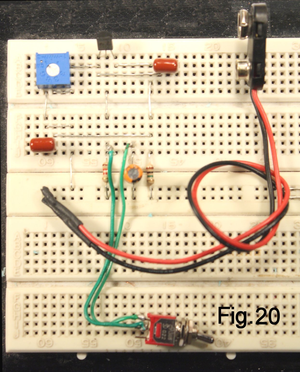
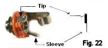
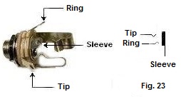
In a typical pedal build, we would use a stereo jack for the input and connect the ring contact to switch battery power. To keep things simple here, we use only the tip and sleeve. Solder a short length of shielded cable to each jack, making sure that the shield is soldered to the sleeve. (Ordinary insulated wire will work, but shielded cable reduces some of the noise inherent in an open layout like this.) Add bare wire terminations to the ends that go to the breadboard just as you did for the battery snap.
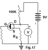
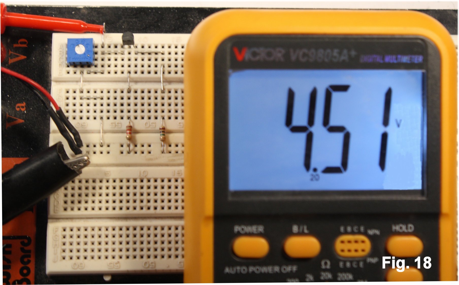
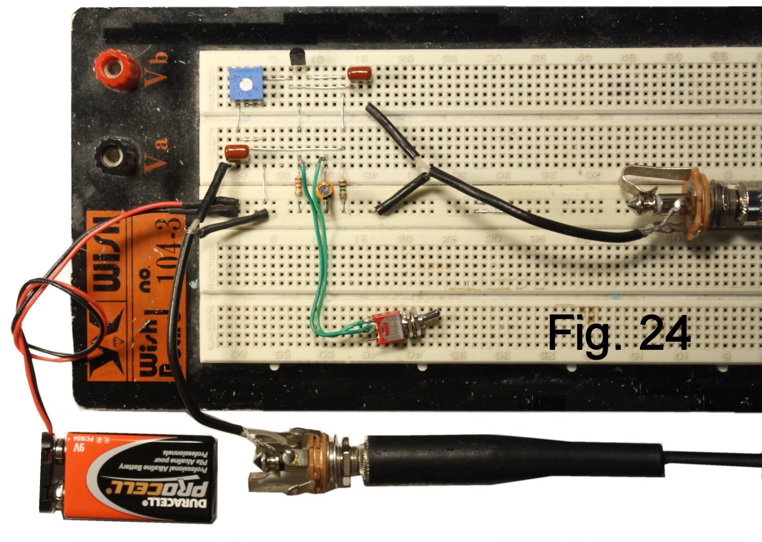
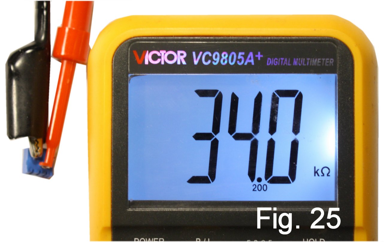
The shields are plugged to the ground bus. Input tip goes to the input capacitor, output tip to output capacitor. Connect your gear with the amplifier set to low volume and connect a battery. Things should look like figure 24, and you should hear a definite clean boost. Flip the switch and make sure that you hear the difference in gain with and without the source bypass cap. You can leave the trimpot in place if you want to be able to tweak further later on. It's also your choice as to whether to set it for 4.5 volts or for maximum volume. I prefer to measure the resistance of the trimpot and find the value of an appropriate fixed resistor. For this device, RD at about 34K puts the Drain at 4.5 volts (Fig. 25). I substituted the nearest 5% value, 33K.
The breadboard kit includes both the trimpot and an assortment of resistors in the range of 10K to 100K.
RD (ohms) x gm (Siemens)
So: 33,000 x .0008 = 26.4
So for a nominal guitar signal of 10 millivolts (.01 volt), we should see something like 260 millivolts at the output.
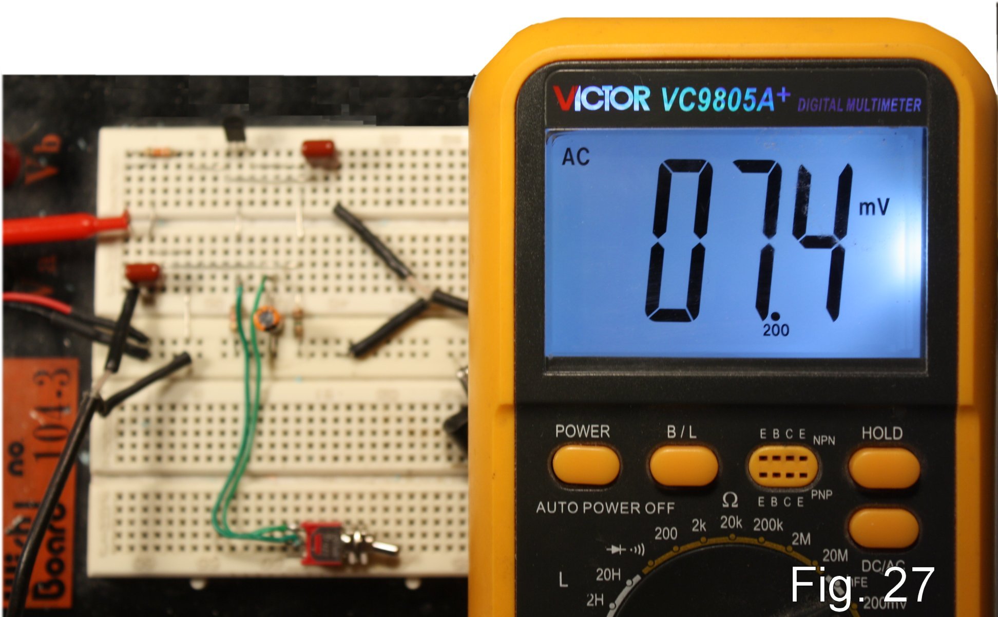
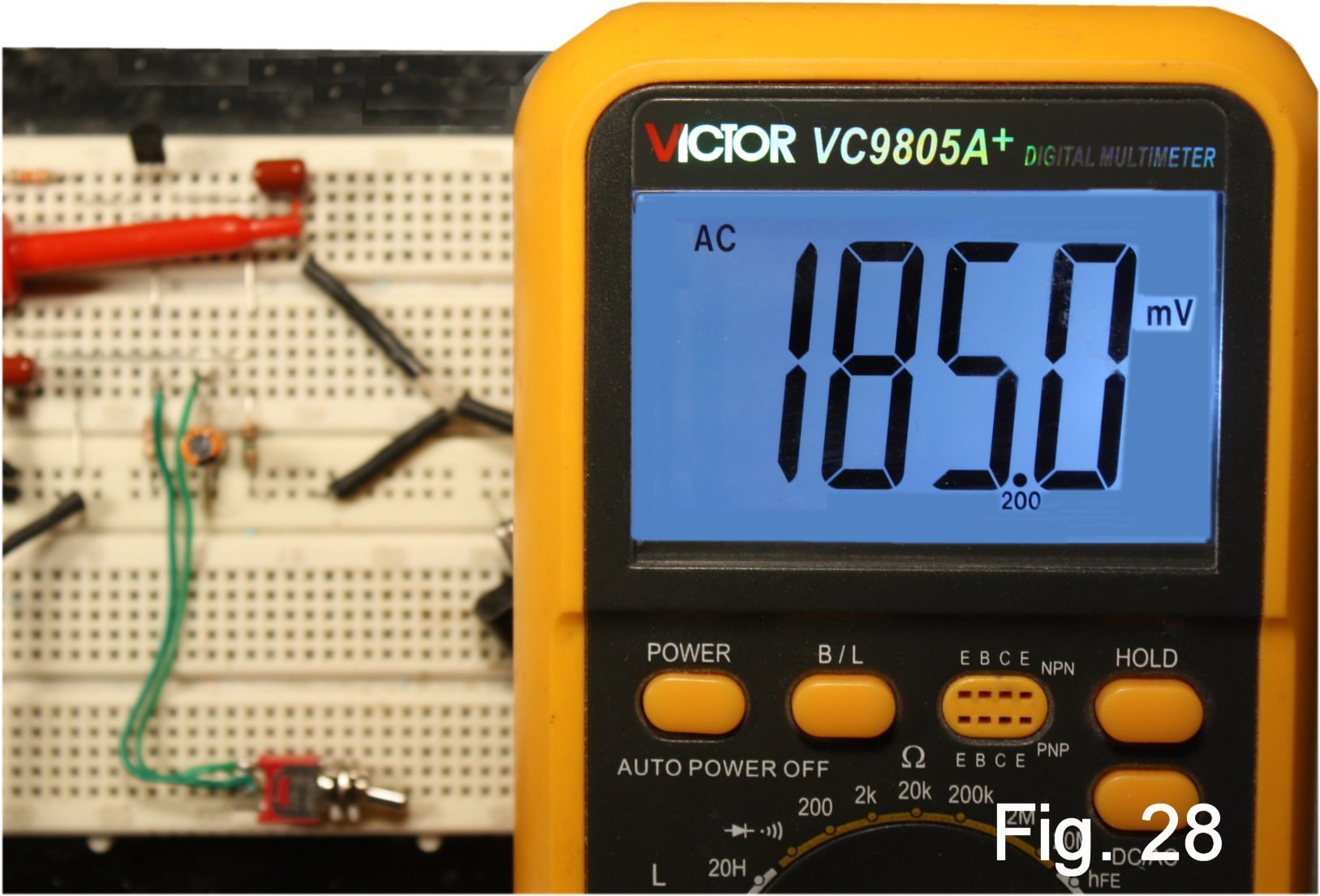
I connected the signal source in place of my guitar and used the AC voltage scale of my multimeter to measure the voltage at input and output (Fig. 27 and 28). 7.4 mv. in, 185 mv. out, factor of 25...Whaddya know, the gain formula is about right!
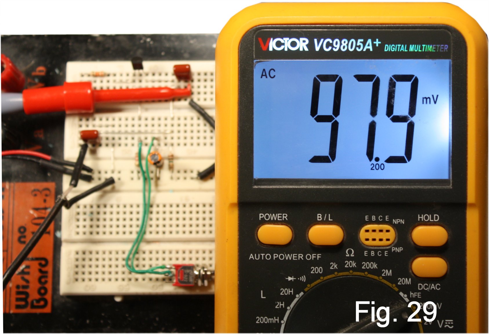
Flipping the switch to take the source bypass out cuts the stage gain by a little less than half (Fig. 29).
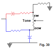
Figure 30 is the basic schematic for the tone stack that is used in many popular pedals, like the E-H Big Muff and the BOSS DS-1. It's simple and effective, and it gives a good sweep from bass to treble with a single pot. The capacitor and resistor in red form a high-pass filter, and the resistor and cap in blue bleed treble to ground. So what gets through the tone stack depends on the position of the wiper of the tone pot.
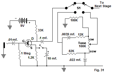
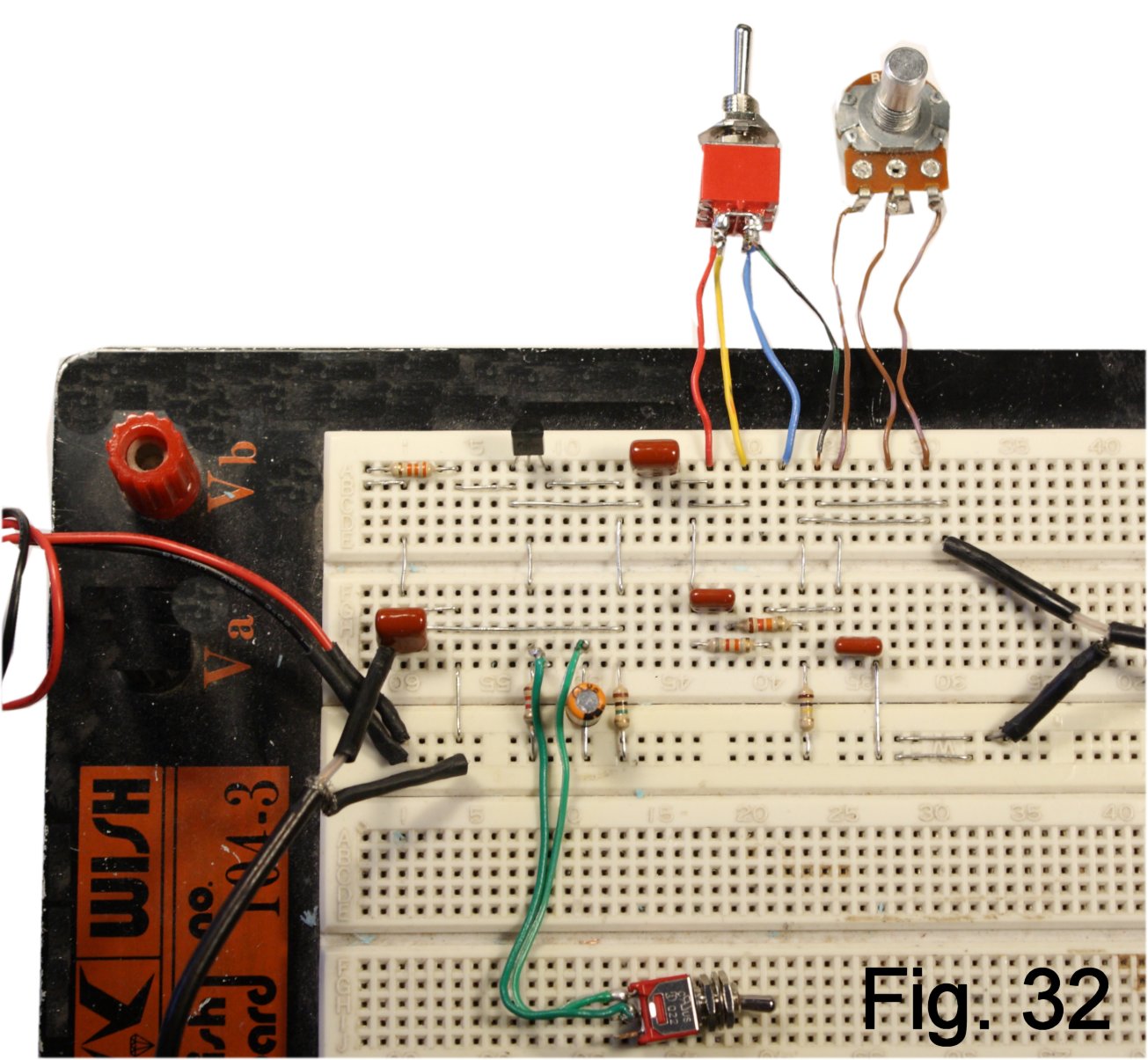
I asked Paul Reid (PRR of diystompboxes.com) for help with setting the R-C values of the tone stack, and he was most generous with advice. Especially, he suggested higher resistances to match the input load. He also directed me to the Duncan Tone Stack Calaculator, which is a great tool for experimenting with the profile of this section. Figure 31 shows the schematic with my chosen component values and bypass switch, and Figure 32 shows the added components on the breadboard.
I tested this much by connecting the output jack tip to the output contact of the bypass switch and verifying that the bypass and the tone control worked properly.
A basic JFET design rule for avoiding distortion is that the input signal voltage to the Gate must not exceed Vp. I presumed a nominal 10 millivolt input signal to the first stage, but peaks may be several times higher depending on who's playing and how hot the pickups are. Vp for the first-stage device was .43 V. Now figure input peaks of 30-50 millivolts and overall gain of 10 through the tone stack...Vp needs to be much higher for the second stage. So I sorted a bunch of parts and came up with one that had these specs:
IDss = .72 ma. Vp = .936 V gm = .875 ms
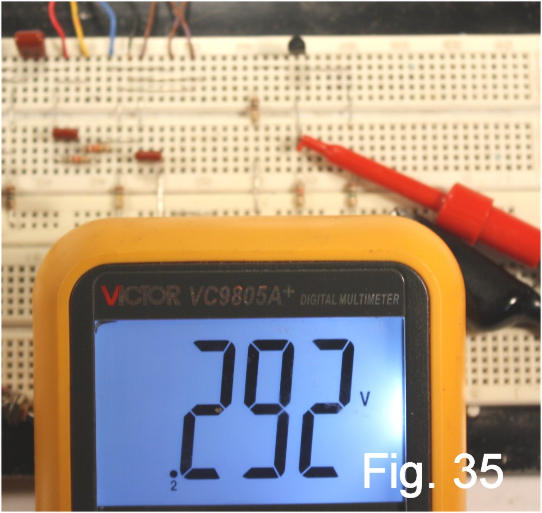
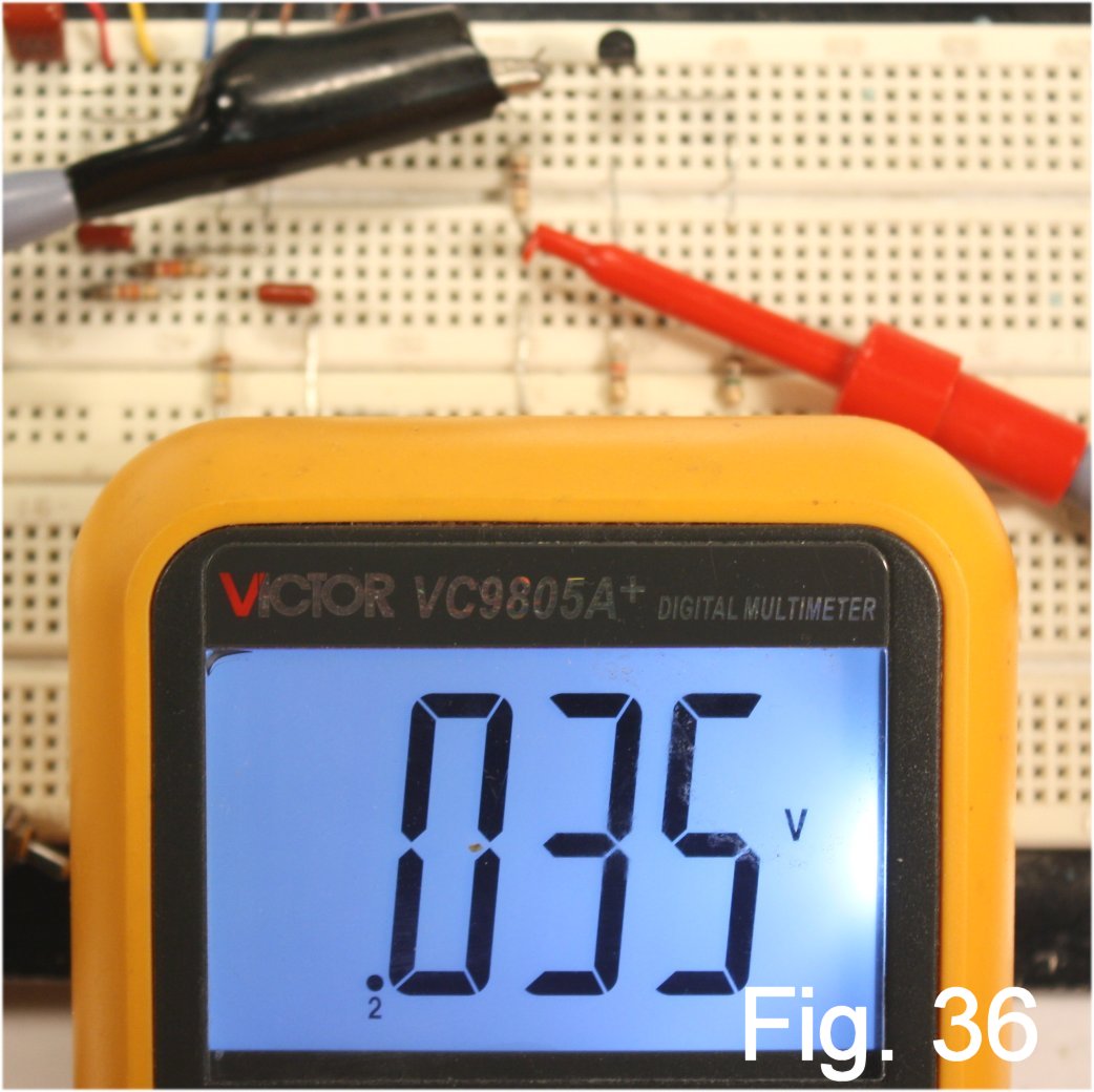
This device will boost about as much as the other one, but it will tolerate a much larger input signal. Once again, I measured the bias voltage that would set the Drain current to 50% of IDss, or .36 ma. For this device it was .296 V, so the Source resistance RS = E/I = .296 / .00036 = 822 ohms. I stuck an 820 ohm resistor in there, and Ohm's Law rules again (Fig. 35, Fig. 36):
The breadboard kit contains an assortment of resistors for biasing the source.
AV (symbol for voltage gain) = RD (ohms) x gm So 10 = RD (ohms) x gm Solving for RD: 10 / .000875 = about 11.4K. I'm going to try 11K and see what the input and output voltages look like.
If you are following these procedures on your breadboard, you can either:
- Do the arithmetic above based on the gain you choose and the gm of your device to get a value for RD, or
- Insert a trimpot, set it to a value that puts 4.5 Volts on the Drain, measure the resistance and substitute a fixed resistor.
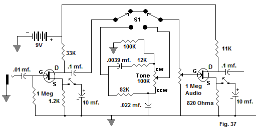
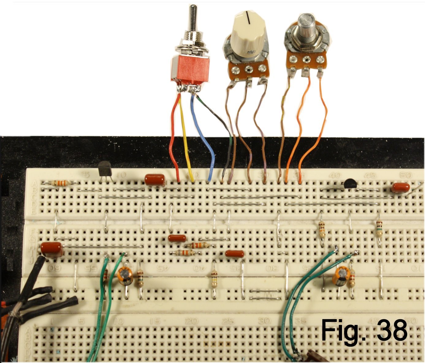
I'm putting a 1 Meg level pot at the input to give me control of the signal level going into the recovery stage (Fig. 37, Fig. 38).
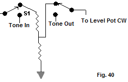
Paul Reid suggests inserting a "pad" that equalizes the input to the second stage when the tone stack is bypassed (Fig. 40). He suggests 300K to 470K on top and 100K to 220K on bottom depending on how much attenuation turns out to be needed. I did not breadboard this, but I will leave room for it when laying out a board.
Where To Go From Here
In the article that will follow this one, I will show how to wire the circuit on perfboard and create a finished pedal in the Bare Box #1. I hope you enjoyed learning to use the breadboard, and that you will use your new skills to hack into other designs and try out your own ideas.
A Parts List
Here is everything needed to do all of what I have described, including the LED demo in the intro article.
| Quantity | Description | SBE Stock List SKU |
| Resistors - All 1/4-watt 5% Carbon Film | ||
| 1 | 100 Ohms | 0900, 0901, etc. |
| 1 | 10K | |
| 1 | 12K | |
| 1 | 82K | |
| 1 | 100K | |
| 1 | 1 Meg | |
| 1 | Source Resistor Bag: 240 ohms to 1.5K (17 values) | |
| 1 | Drain Resistor Bag: 2K to 100K (41 Values) | |
| Potentiometers and Trimmers | ||
| 1 | 100 K Linear | 1005A |
| 1 | 1 Meg Audio | 1005A |
| 1 | 100K Cermet Trimmer | 1015 |
| Capacitors | ||
| 1 | .0039 mf. 50 Volt Polyester Film | 1101B or 1150 |
| 2 | .022 mf. 50 Volt Polyester Film | |
| 1 | .01 mf. 50 Volt Polyester Film | 1101B or 1150 |
| 2 | .1 mf. 50 Volt Polyester Film | |
| 2 | 10 mf. 16 Volt Radial Electrolytic | 1400 |
| 1 | 47 mf. 16 Volt Radial Electrolytic | |
| Transistors and Diodes | ||
| 2 | Selected JFETs | |
| Wire and Tubing | ||
| Bare Tinned Copper Wire, #22 or #24 | 0509 | |
| Insulated Tinned Copper Wire, #22 or #24 | 0508M | |
| Shielded Cable | 0510 | |
| 1/16" heat shrink | 0500 | |
| Jacks, Fittings, Switches | ||
| 1 | Mono Jack, Switchcraft #11 | 0600 |
| 1 | Stereo Jack, Switchcraft #12B | 0602 |
| 1 | 9-Volt Battery Snap | 0619 |
| 2 | Sub-miniature SPST Toggle Switch | 0222 |
| 1 | Sub-miniature DPDT Toggle Switch | 0223 |
| Tools | ||
| 1 | Breadboard or Breadboard Strip | 2700, 2700A, 2700B |
| 1 | Multimeter | 2701, 2701A |